Company news / Oct 2026
Planck Semicon presents integrated semiconductor inspection and metrology solutions at WESEMiBAY 2026
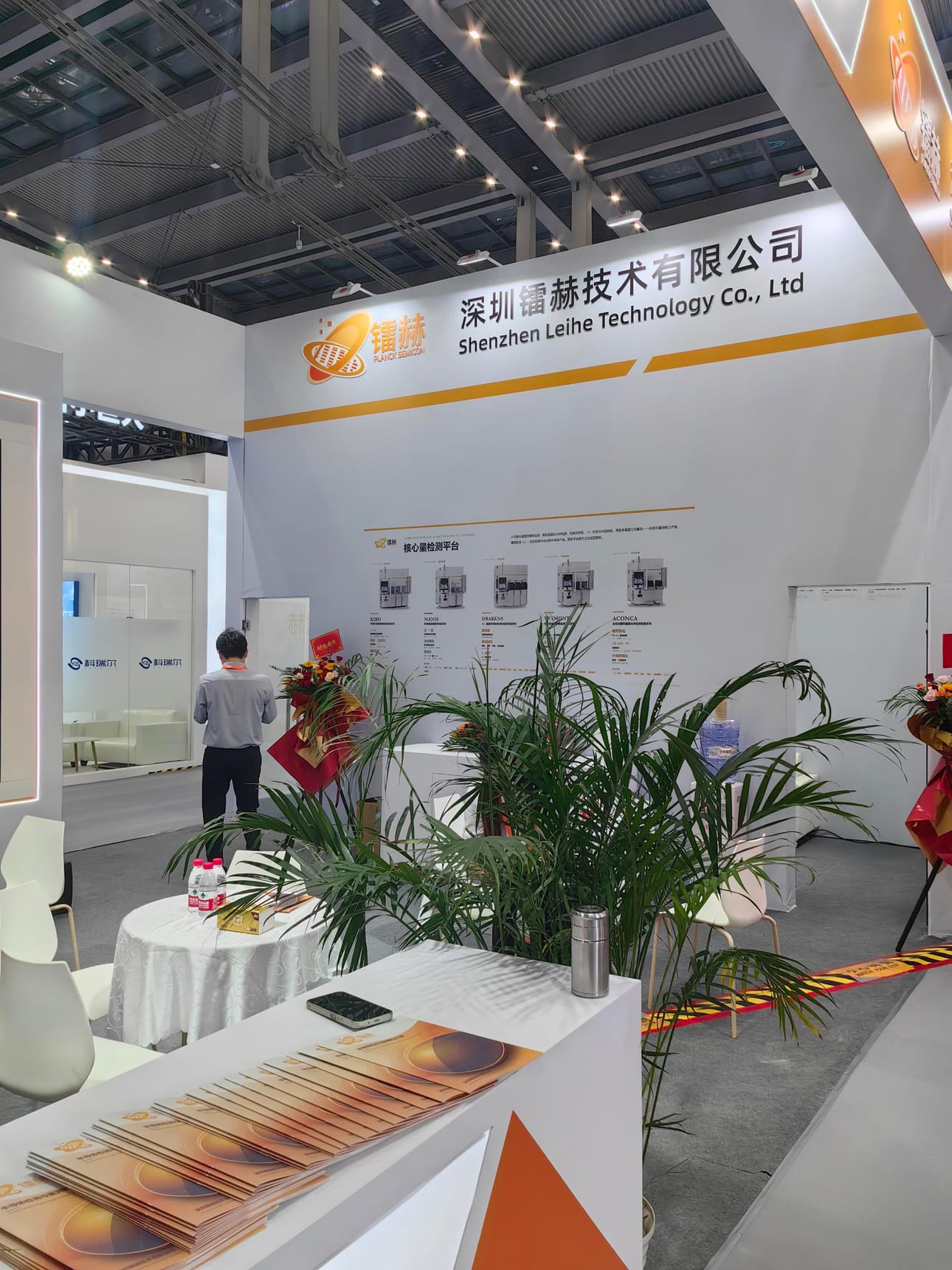
At Booth 8F35 in the Shenzhen Convention & Exhibition Center (Futian), Planck Semicon presented its solutions for semiconductor defect inspection and precision metrology and met visitors on site.
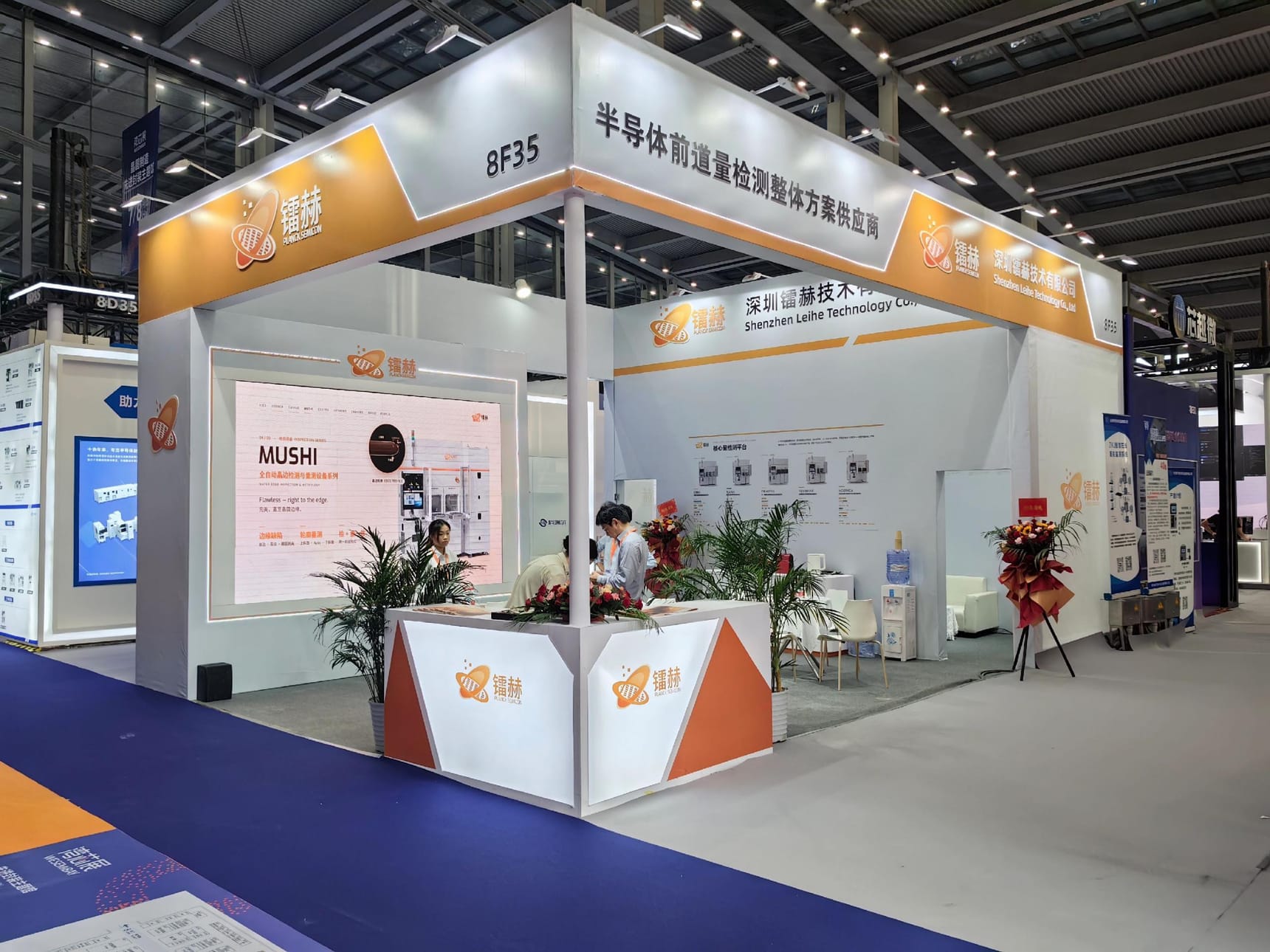
From October 14 to 16, 2026, the Bay Area Semiconductor Industry Ecosystem Expo (WESEMiBAY 2026) took place at the Shenzhen Convention & Exhibition Center (Futian). Planck Semicon exhibited at Booth 8F35, presenting its product solutions for semiconductor defect inspection and precision metrology and meeting visitors face to face.
This year’s expo spanned wafer manufacturing, compound semiconductors, advanced packaging and IC design / AI infrastructure, giving companies across the supply chain a platform to showcase technology and connect supply with demand. Planck Semicon used the occasion to share with industry partners its approach to inspection and metrology across different materials, structures and process steps.
At the booth, product visuals, solution boards and product brochures laid out Planck Semicon’s portfolio in wafer defect inspection, wafer edge inspection and metrology. The MUSHI series covers wafer edge defect inspection and edge profile metrology, while the ACONCA series provides automated optical inspection of patterned wafers, helping engineering teams observe and assess process conditions from different angles.
Alongside its equipment, the company showed PlanckADC, its intelligent defect classification and yield management platform. From inspection data and automatic classification to statistical analysis and result tracking, Planck Semicon’s focus goes beyond finding defects: it is about turning inspection results into process information that can be reviewed, analyzed and tracked over time.
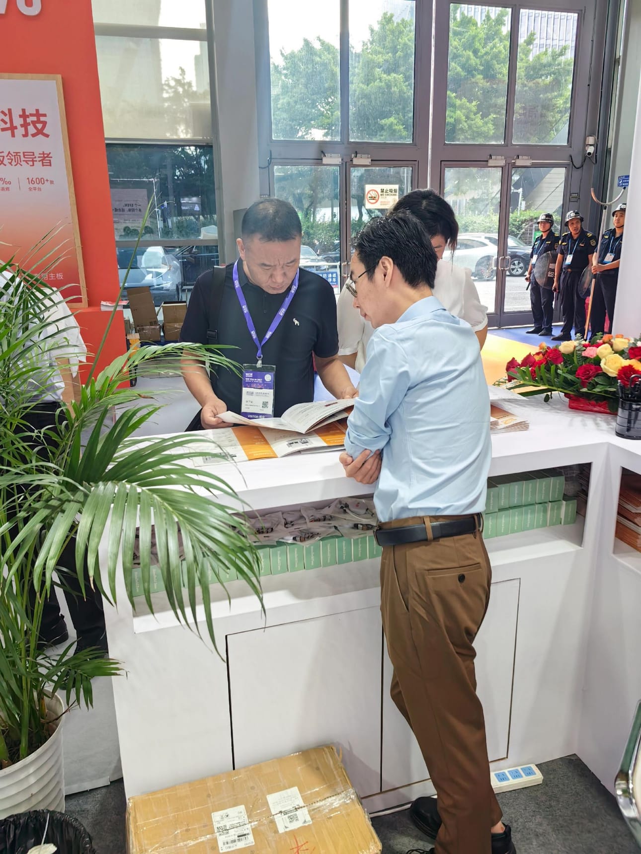
Throughout the show, the Planck Semicon team walked visitors through the product materials, explaining capabilities and target applications. In inspection and metrology, the right solution depends on the material, the defects of interest, the measurement parameters and the conditions on the production line. Face-to-face conversations made it possible to map each product to specific application questions.
Planck Semicon thanks the customers, partners and industry peers who visited its booth. The company will continue to advance product development and application exchange around the inspection and metrology needs of semiconductor manufacturing and advanced packaging, giving engineering teams a firmer basis for process decisions.