
Platform series no. 06/ 09
INSPECTION SERIES
VEYMONT Series
Full-Surface Nano-Topography Inspection System Series
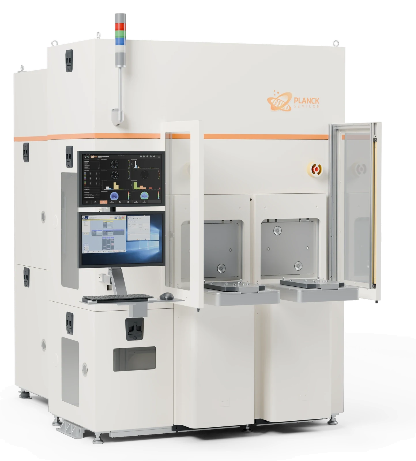
Reveal the invisible.
- 2 nmNano-topography · Vertical precision
Dislocation cracks · Epi steps · Process marks · Dimples
- Front + backDual-side simultaneous scan
Single load · Production-rate throughput
- Bonding voidsNon-contact · Can replace CSAM
No couplant · Full wafer in one pass
01PRODUCT INTRODUCTION
Overview
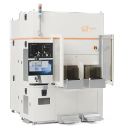
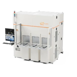
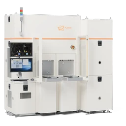
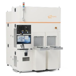
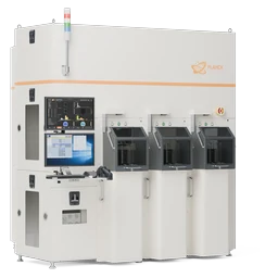
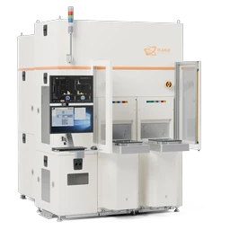
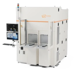
VEYMONT images the entire front and back surfaces of a wafer at nanoscale, with vertical precision down to 2 nm. It reveals dislocation cracks, epitaxial steps, grinding / CMP marks and local dimples that conventional bright-field and dark-field optics cannot see, capturing substrates and epi wafers completely in a single imaging pass. In advanced packaging it inspects bonding voids across the full wafer without contact and can replace CSAM ultrasonic scanning. Used on production lines for silicon wafers, SiC / GaN epi and thinned IGBT backsides.
Inspection targets
- Dislocation cracks
- Epi steps
- Grinding / CMP marks
- Local dimples
- Bonding voids
Applications
- Silicon / SOI wafers
- Hybrid / temporary bonding voids
- SiC / GaN epi
- Thinned IGBT backsides
- CMP process monitoring
02PRODUCT FEATURES
Key features
Nano-topography in clear view
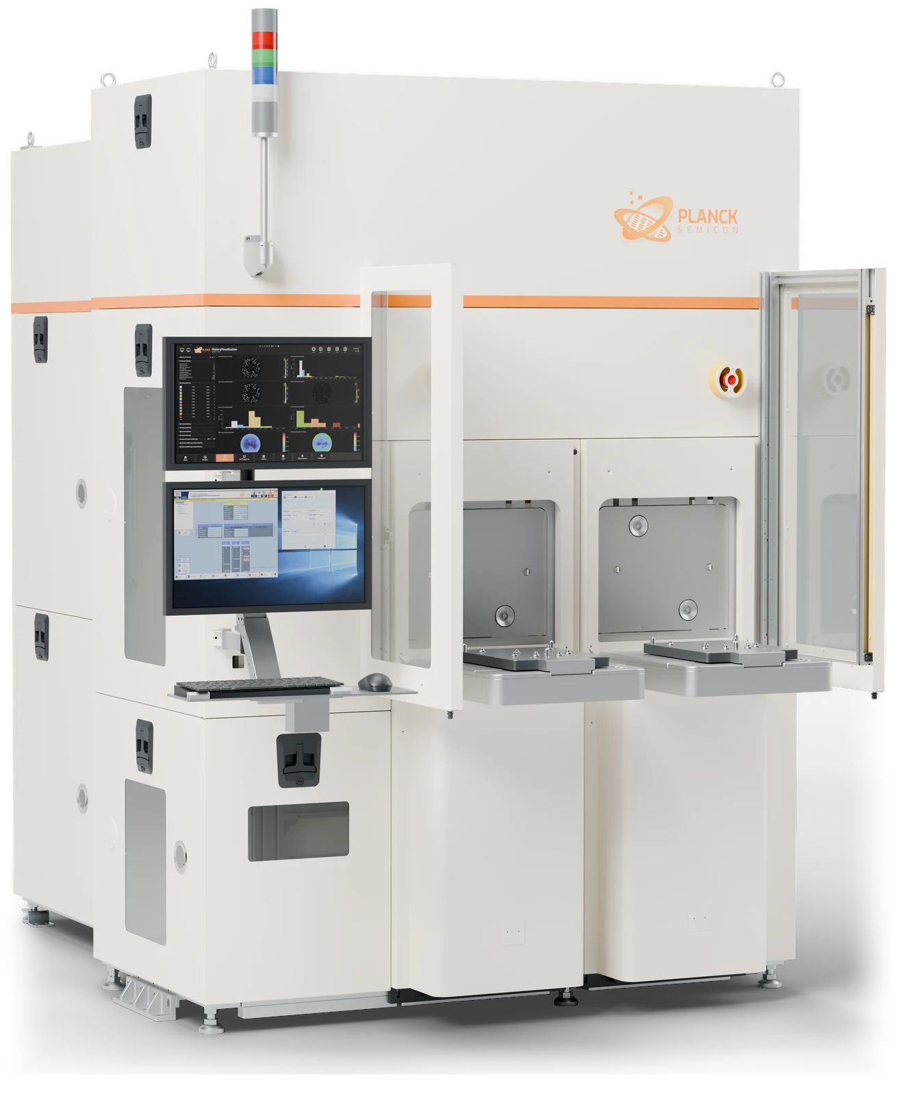
Dislocation cracks, epitaxial steps, grinding / CMP marks and local dimples on substrates and epi wafers, captured in a single imaging pass.
Non-contact bonding-void inspection
Bubbles and voids in hybrid and temporary bonding detected across the full wafer with no couplant: a replacement for CSAM ultrasonic scanning.
Front and back in one scan
Full dual-side coverage from a single load, with height maps, roughness and local flatness reported together.
PLANCKADC · Yield-management ready
Results flow straight into PlanckADC
AI classification and grading, result monitoring with SPC, and Wafer Map traceability, connected to your MES / YMS.
About PlanckADC03MORE SYSTEMS
Other systems
- KIBO SeriesUnpatterned Wafer Defect Inspection SystemInspection
- ACONCA SeriesFully Automatic Patterned Wafer Optical Inspection SystemInspection
- CANIGO SeriesAutomatic Wafer Backside Inspection SystemInspection
- MUSHI SeriesAutomatic Wafer Edge Inspection & Metrology SystemInspection
- CARPPA SeriesFast Inline Process Control SystemInspection
- DRAKENS SeriesSiC Wafer Surface & Crystal Defect Inspection SystemInspection
- NANSI SeriesMulti-Channel Wafer Metrology SystemMetrology
- ELBRUS SeriesFull-Wafer Geometry Metrology SystemMetrology
PRODUCT INQUIRY
Discuss yourprocess needs
We match a platform to your material, process step and the parameters you care about.
- SalesProducts and commercial inquiriessales@plancksemicon.com
- GeneralCorporate affairs and partnershipsinfo@plancksemicon.com
- Head office
- 11/F, Block B, Long Guang Century Building, Bao’an Center, Bao’an District, Shenzhen, China
- Phone
- +86-755-21063549