
Platform series no. 03/ 09
INSPECTION SERIES
CANIGO Series
Automatic Wafer Backside Inspection System Series
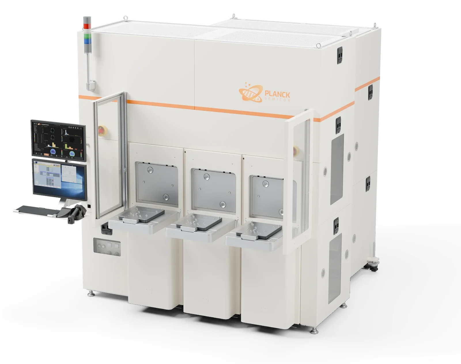
Perfection has another side.
- Single shotThe full backside in one capture
Particles · Scratches · Chips · Stains · Chuck marks
- Recipe-freeReady out of the box
Zero changeover between products
- Non-contactNon-contact handling throughout
No secondary scratches or contamination
01PRODUCT INTRODUCTION
Overview
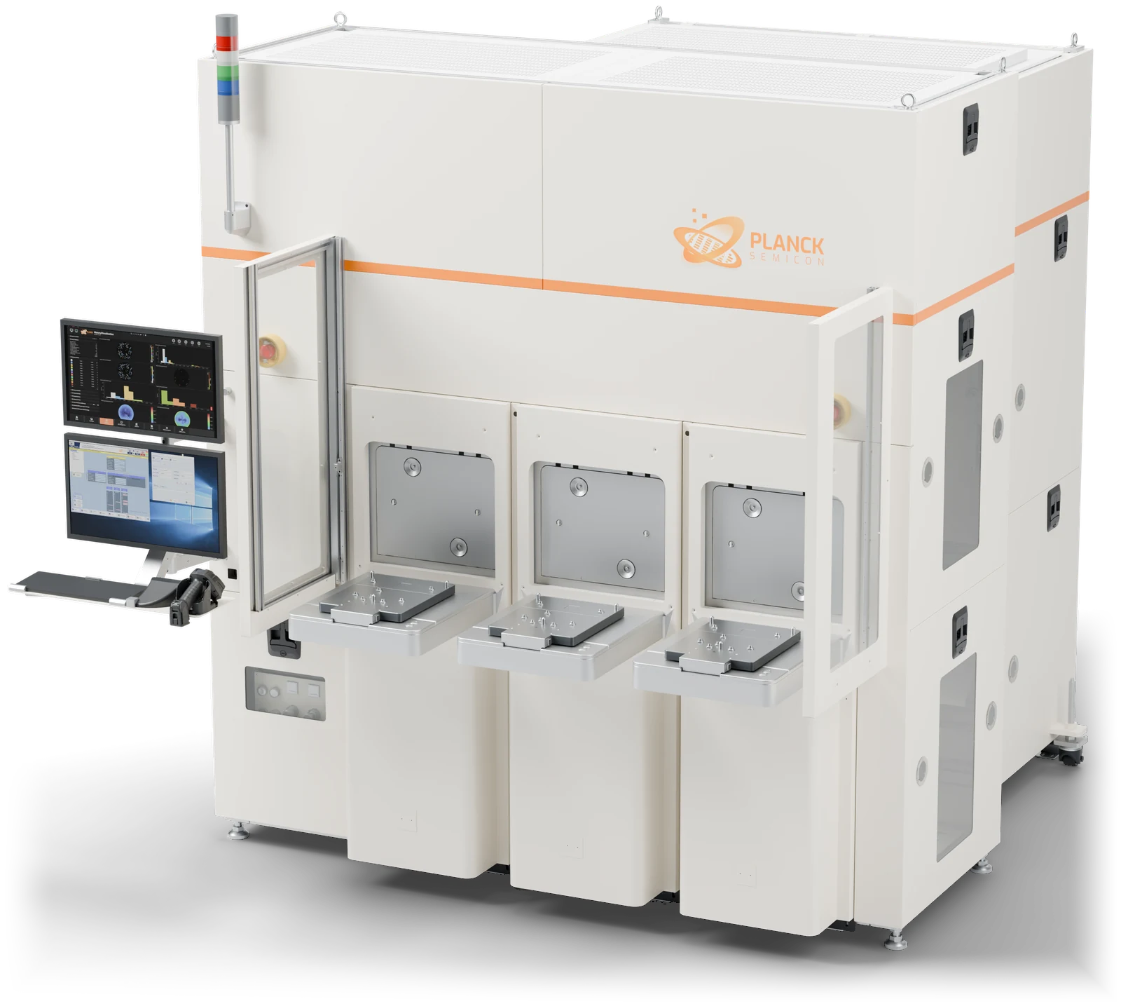
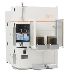
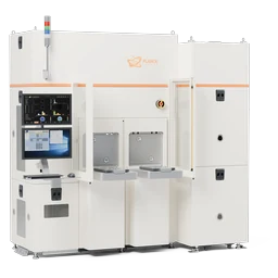
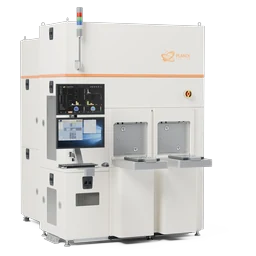
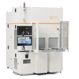
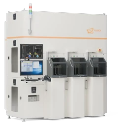
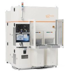
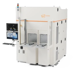
CANIGO is dedicated to the wafer backside. With non-contact handling and single-shot full-wafer imaging, it detects backside particles, scratches, edge chips, stains, residue and chuck marks without product-specific recipes, and runs inline at the same pace as lithography, CMP and other process tools. Used for wafer-supplier OQC, backside cleanliness control before lithography in the fab, thinned wafers, and pre-bond inspection in advanced packaging.
Inspection targets
- Backside particles
- Scratches
- Edge chips
- Stains / residue
- Chuck marks
Applications
- Wafer OQC
- Pre-litho backside control
- Thinned wafers
- Advanced packaging pre-bond
02PRODUCT FEATURES
Key features
One pass, no recipes
The full wafer is imaged in a single shot with no product-specific recipes, so product changes take zero changeover time.
Non-contact throughout
Non-contact backside handling means inspection introduces no secondary scratches or contamination.
Backside control before lithography
Runs inline at the pace of the main tools and stops the backside particles that cause defocus and overlay errors before they reach lithography.
PLANCKADC · Yield-management ready
Results flow straight into PlanckADC
AI classification and grading, result monitoring with SPC, and Wafer Map traceability, connected to your MES / YMS.
About PlanckADC03MORE SYSTEMS
Other systems
- KIBO SeriesUnpatterned Wafer Defect Inspection SystemInspection
- ACONCA SeriesFully Automatic Patterned Wafer Optical Inspection SystemInspection
- MUSHI SeriesAutomatic Wafer Edge Inspection & Metrology SystemInspection
- CARPPA SeriesFast Inline Process Control SystemInspection
- VEYMONT SeriesFull-Surface Nano-Topography Inspection SystemInspection
- DRAKENS SeriesSiC Wafer Surface & Crystal Defect Inspection SystemInspection
- NANSI SeriesMulti-Channel Wafer Metrology SystemMetrology
- ELBRUS SeriesFull-Wafer Geometry Metrology SystemMetrology
PRODUCT INQUIRY
Discuss yourprocess needs
We match a platform to your material, process step and the parameters you care about.
- SalesProducts and commercial inquiriessales@plancksemicon.com
- GeneralCorporate affairs and partnershipsinfo@plancksemicon.com
- Head office
- 11/F, Block B, Long Guang Century Building, Bao’an Center, Bao’an District, Shenzhen, China
- Phone
- +86-755-21063549