

See the unseen defects
Inspection and metrology for front-end fabs and advanced packaging, from incoming substrate to final shipment, built on precision optics, intelligent algorithms and engineering experience.
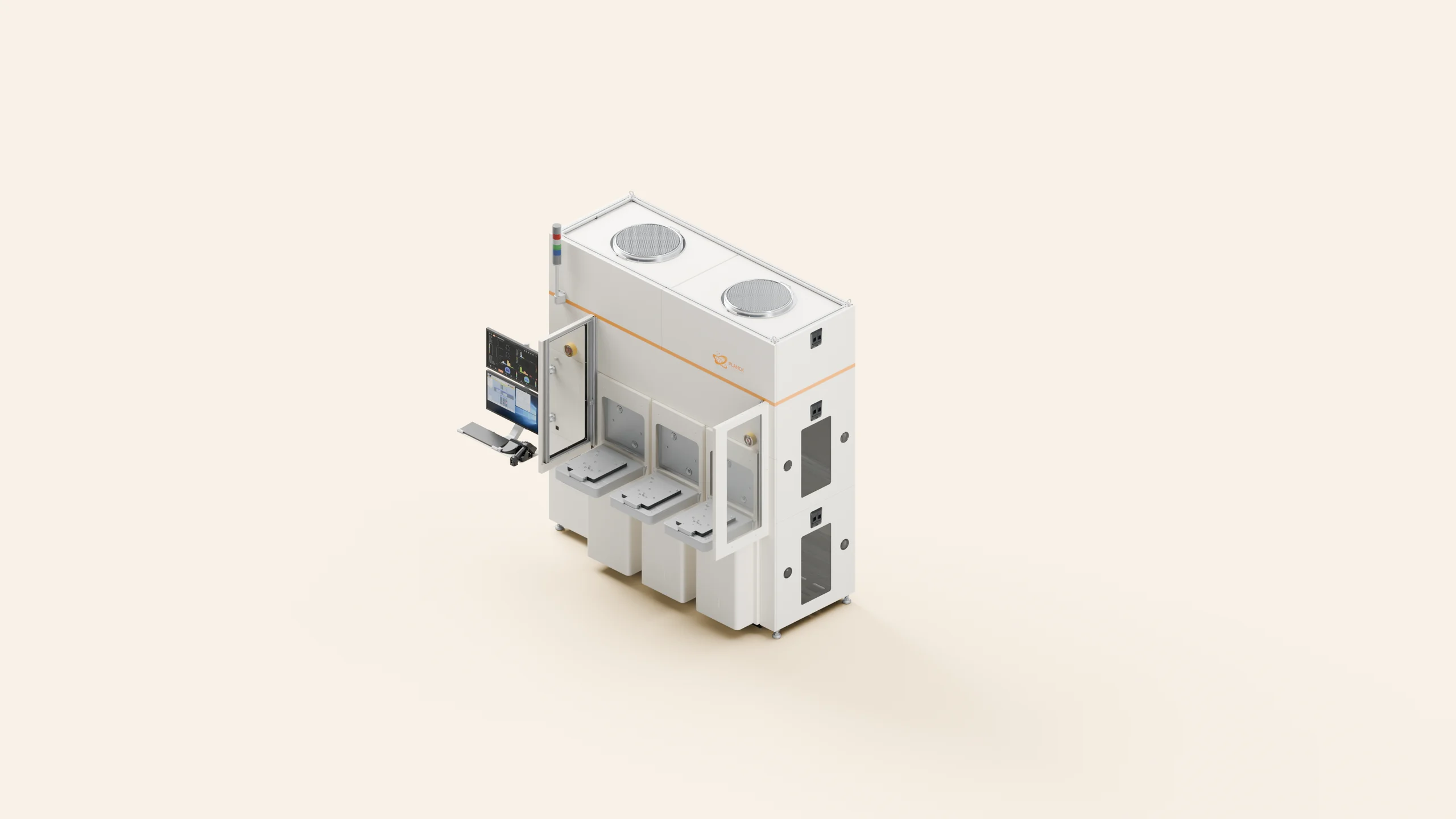
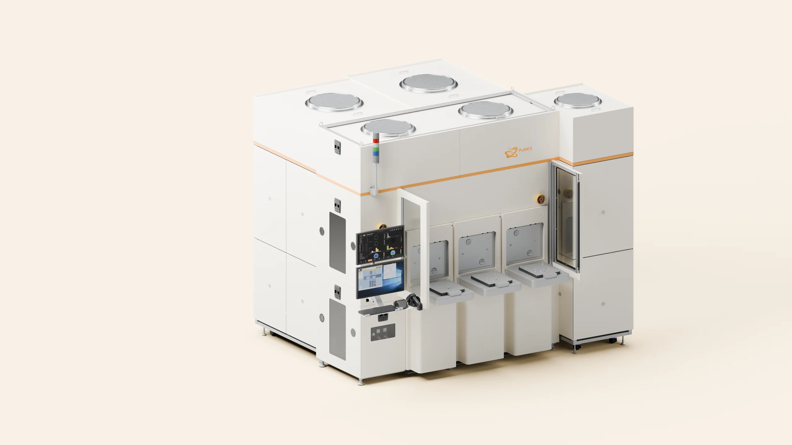
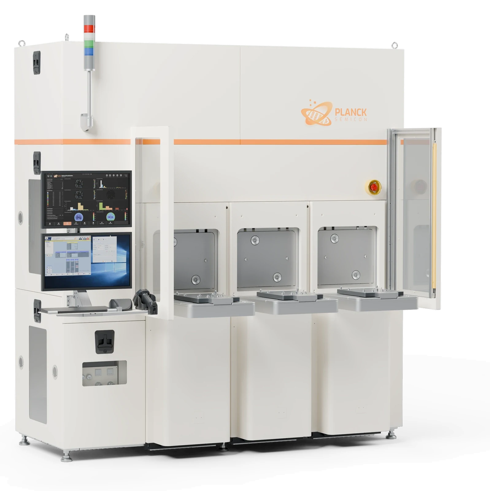
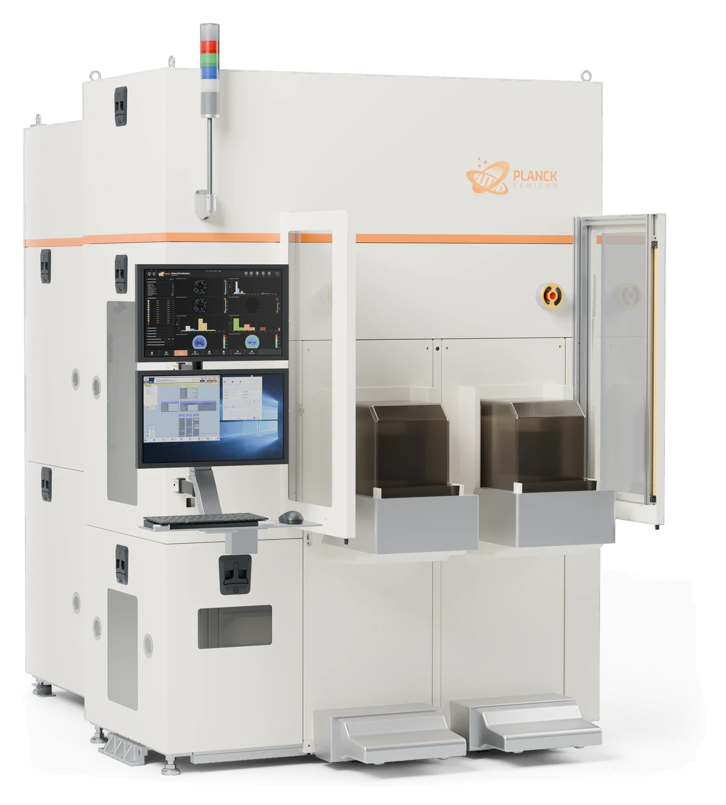
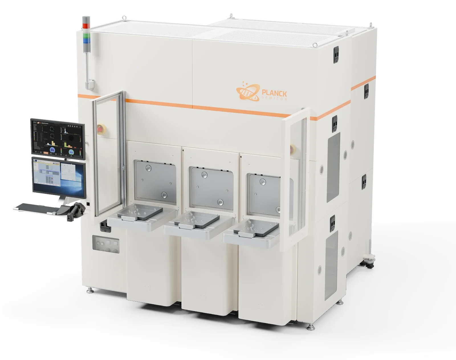
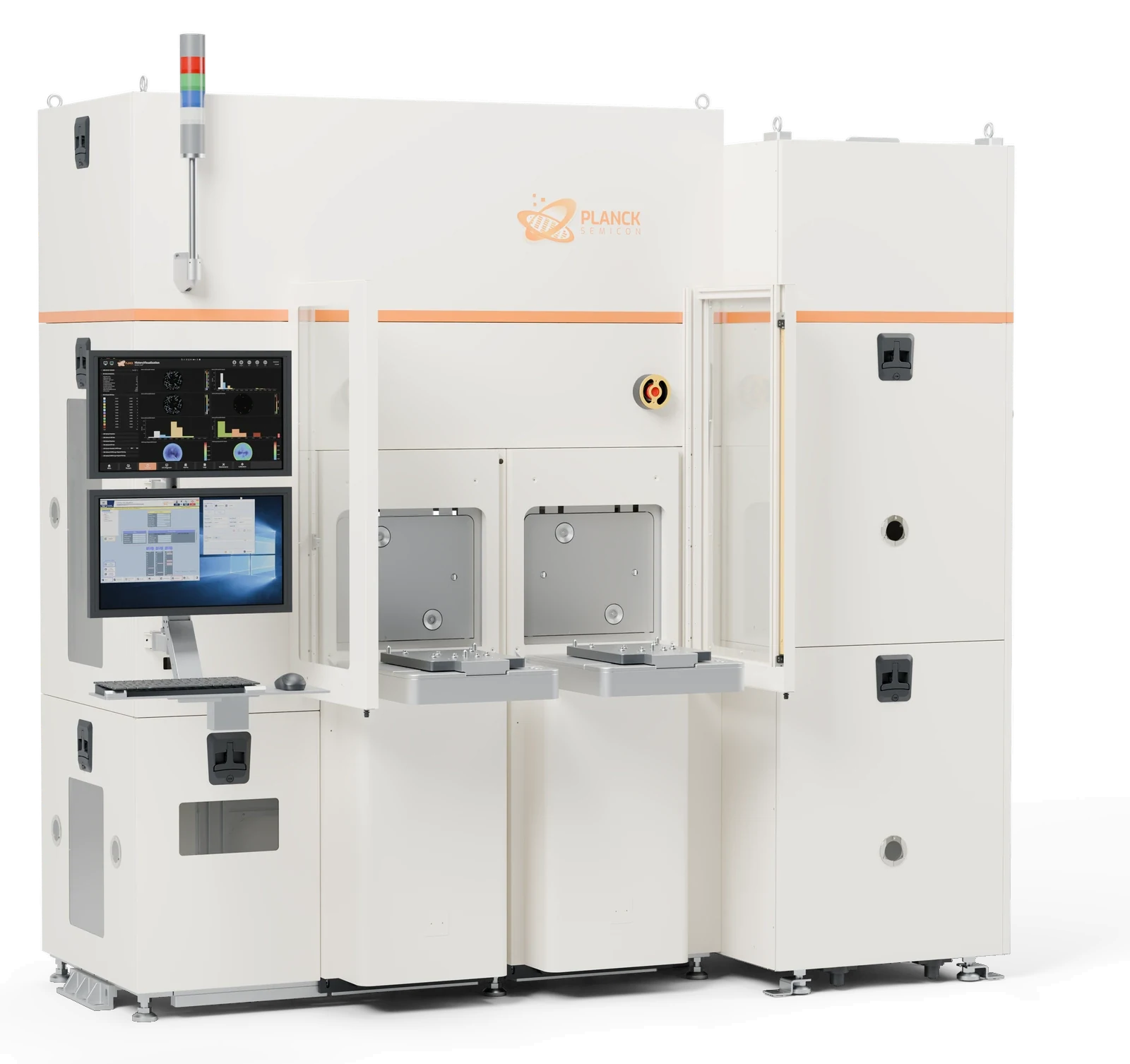
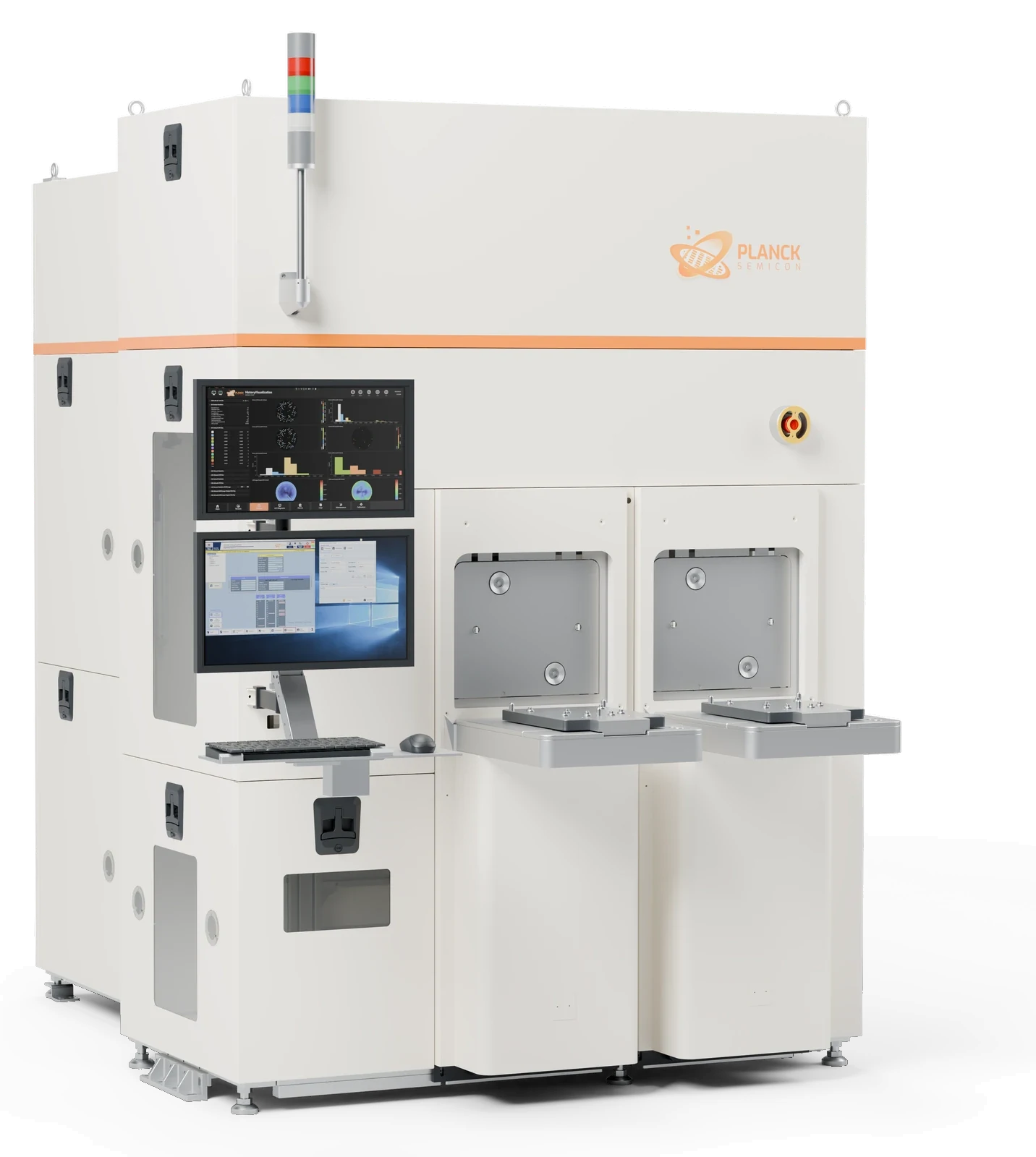
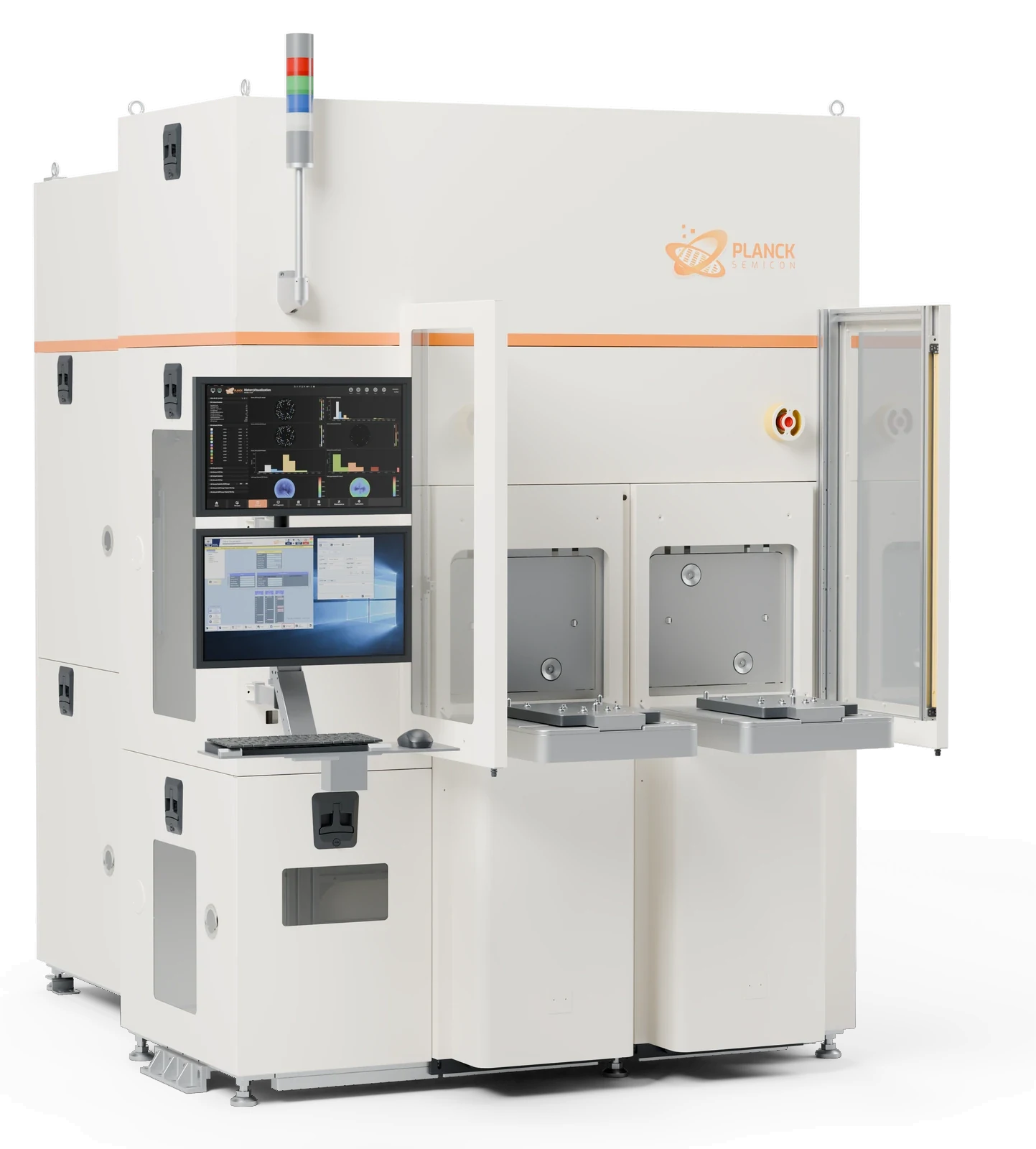
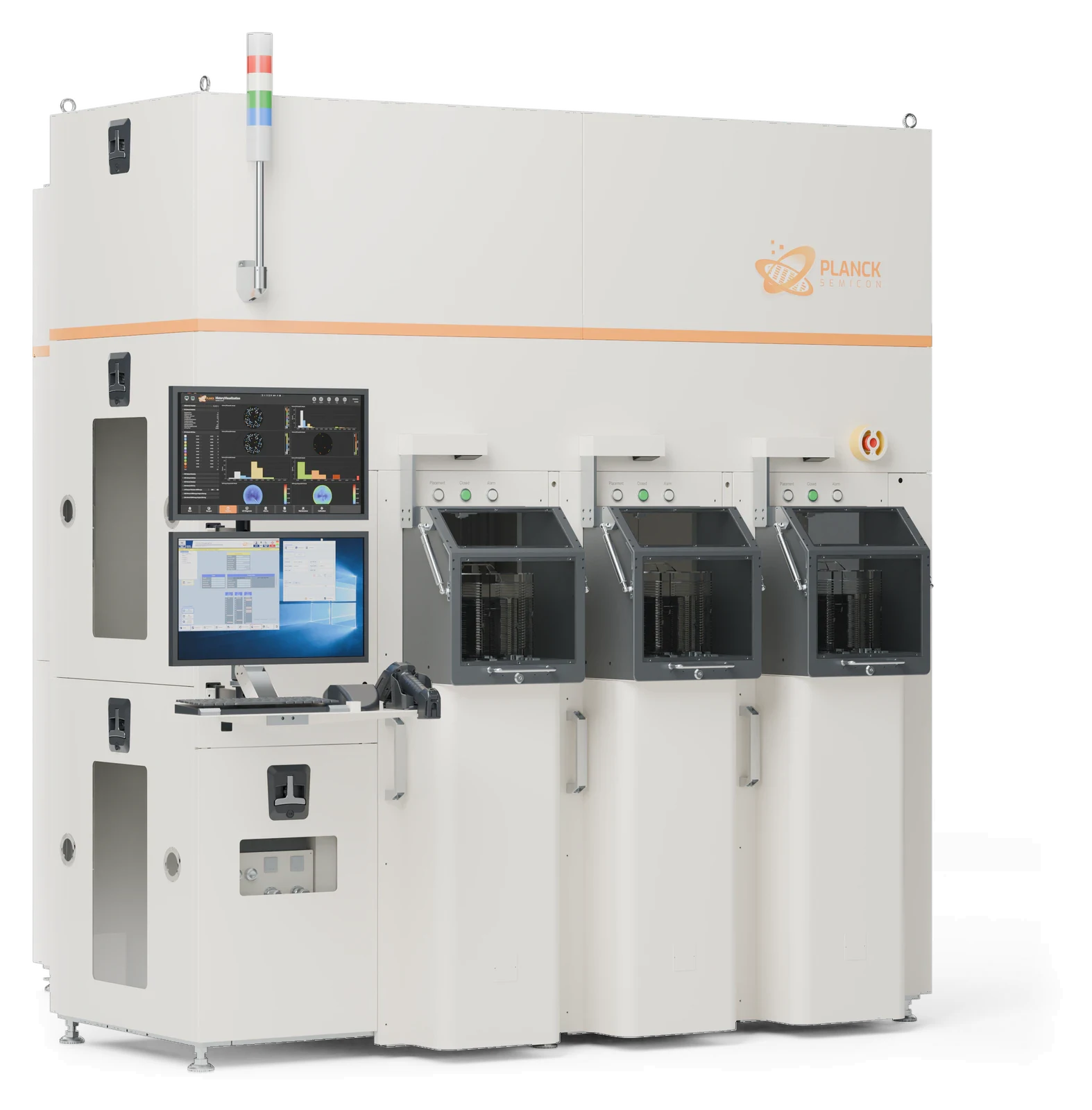
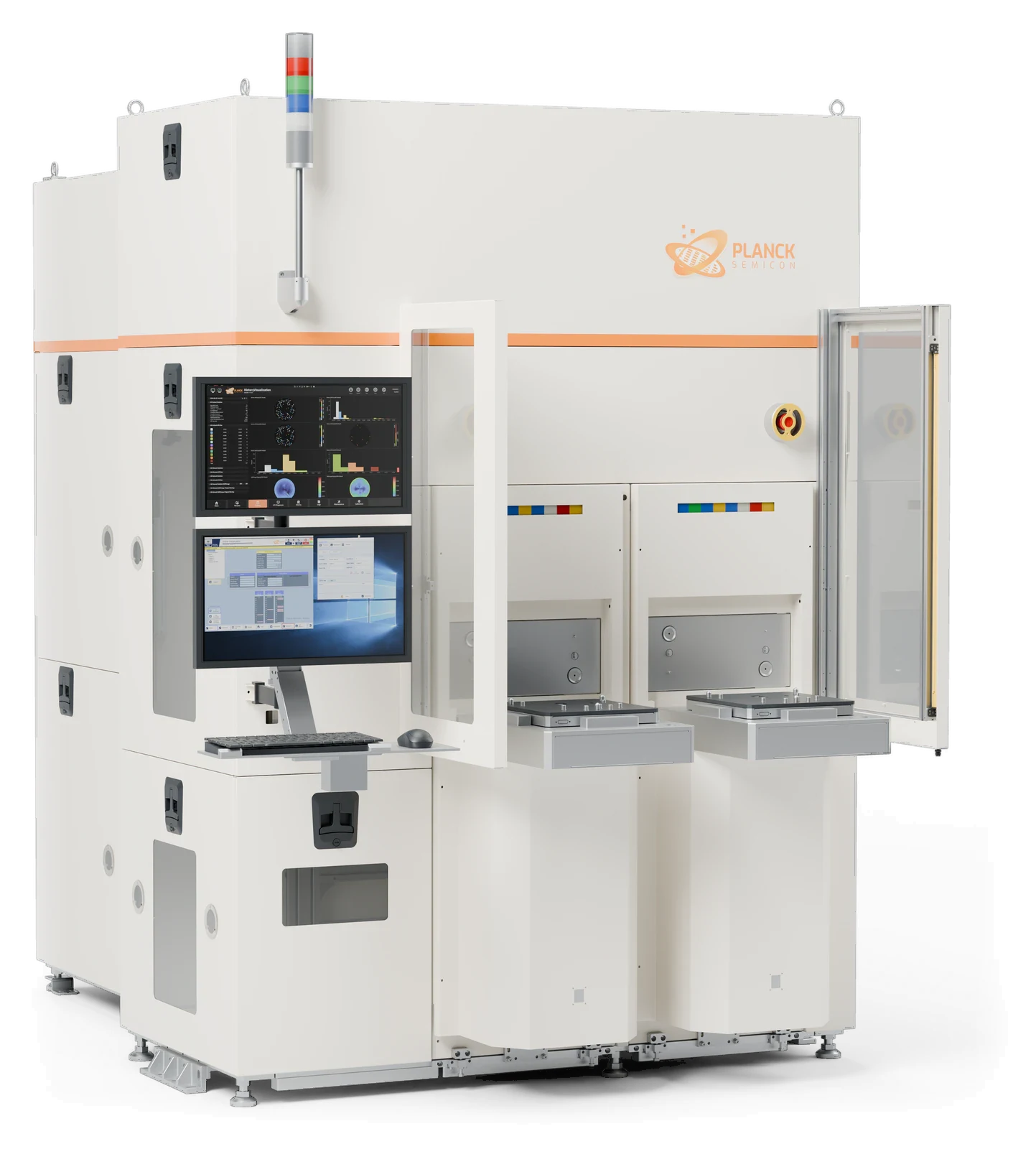
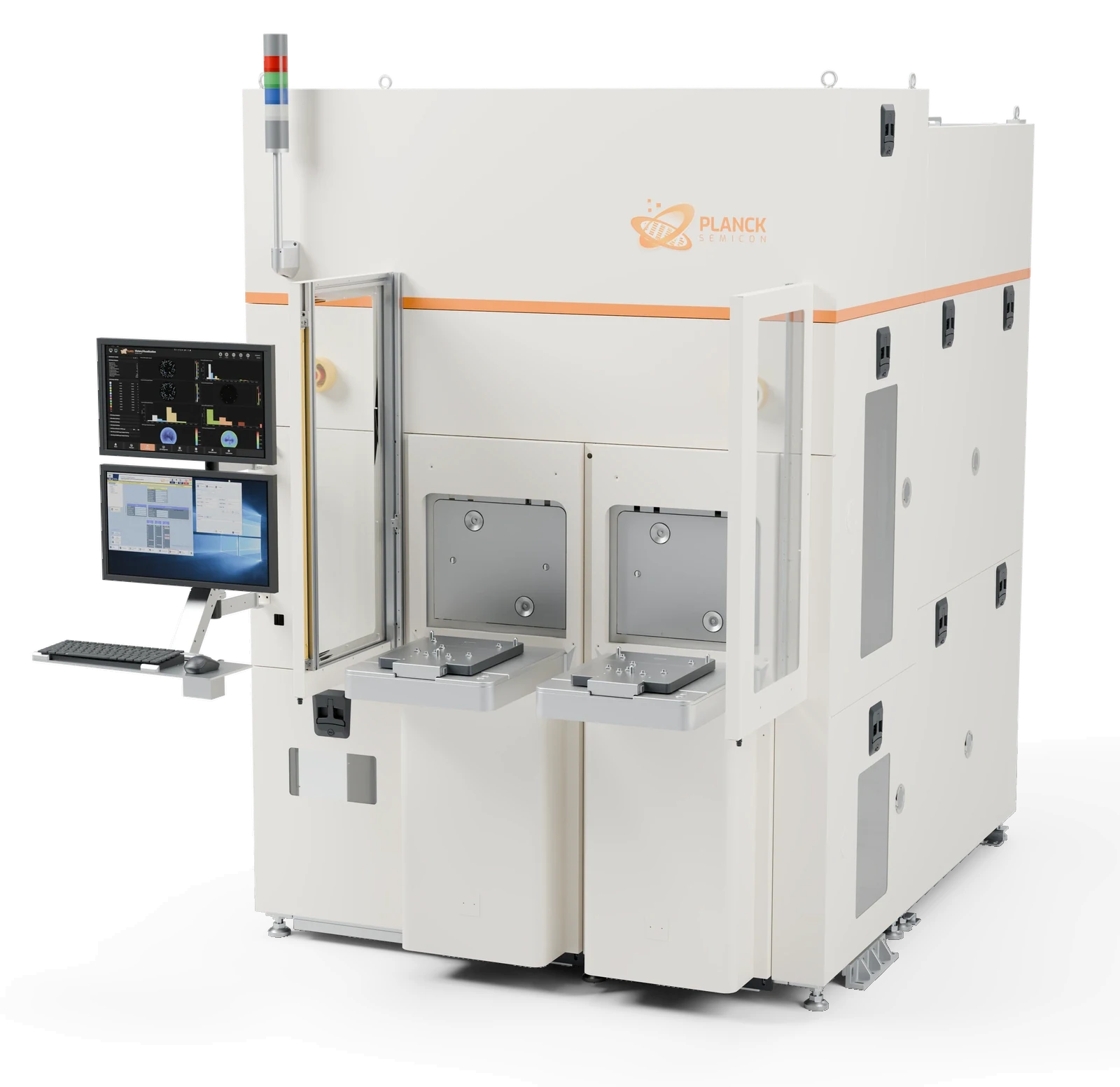
Machine components: Fan filter unit (FFU), Panels (Enclosure), Inspection module (PM), Load port, Wafer handling (EFEM), Operator terminal (HMI).
CORE CAPABILITIES
The invisible,made measurable
BF / DF · PL
Selectable imaging channels
Multi-channel optics
Bright-field, dark-field, PL and multi-band imaging, matched to each material and defect type.
Sub-micron
Minimum TSV / TGV CD
3D precision metrology
Thickness / TTV, Bow / Warp, film thickness and trench depth, all measured without contact.
2 nm
Vertical precision
Full-surface topography
Front and back scanned in one pass, revealing dislocations, cracks, epi steps and bonding voids.
MES / YMS
Direct data integration
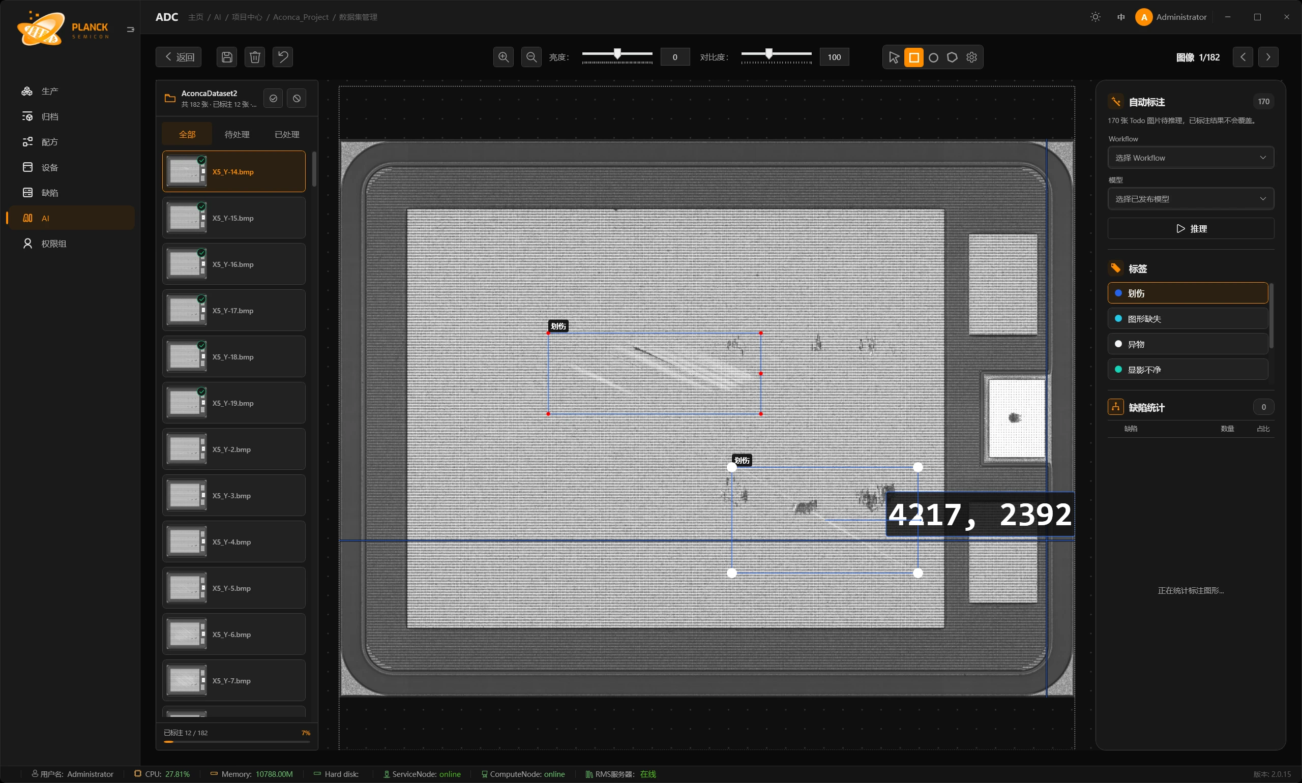
Automatic defect classification
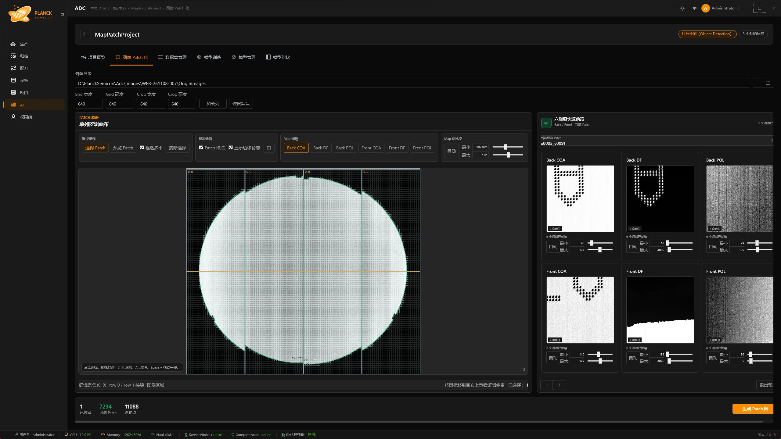
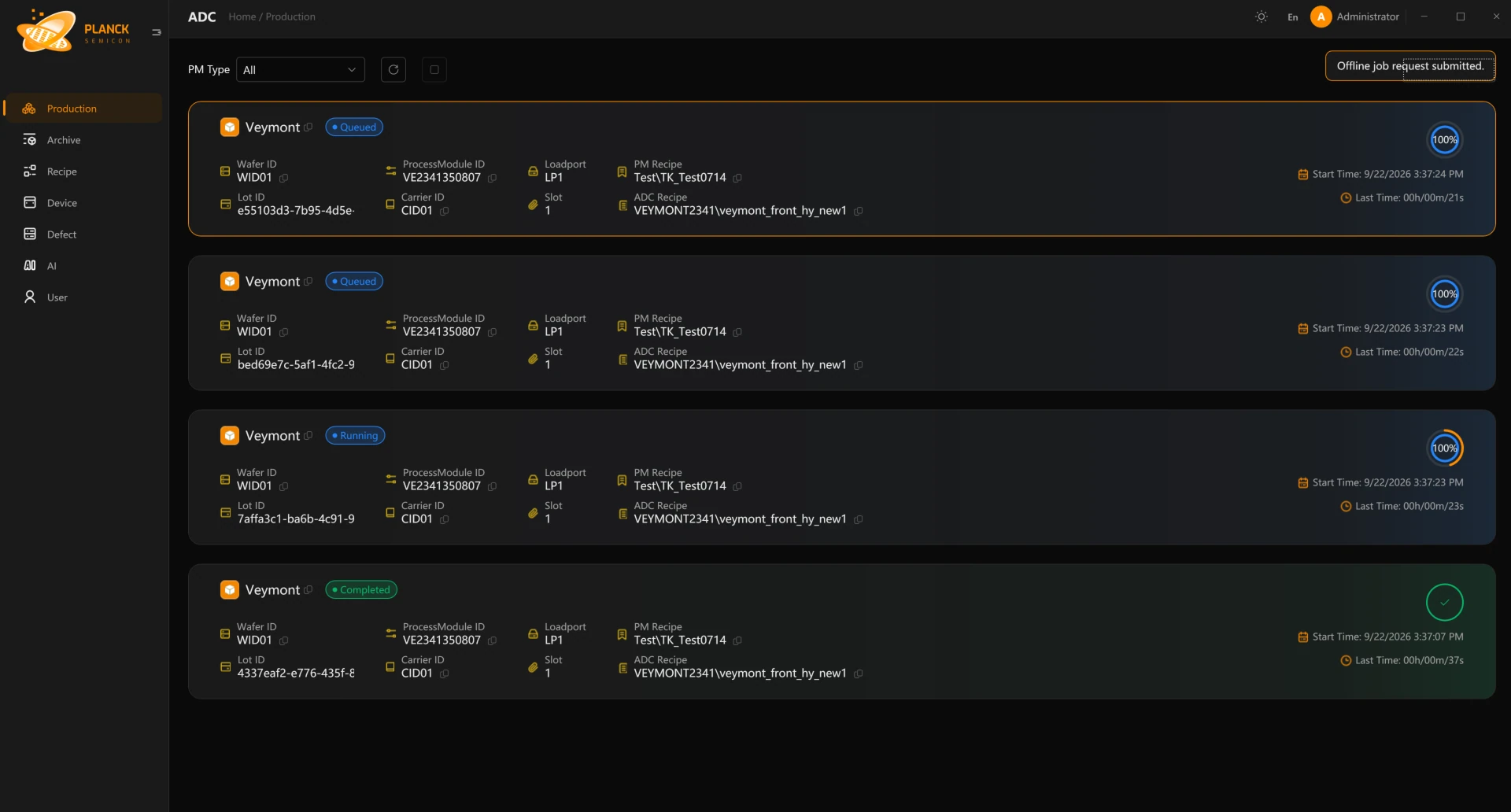
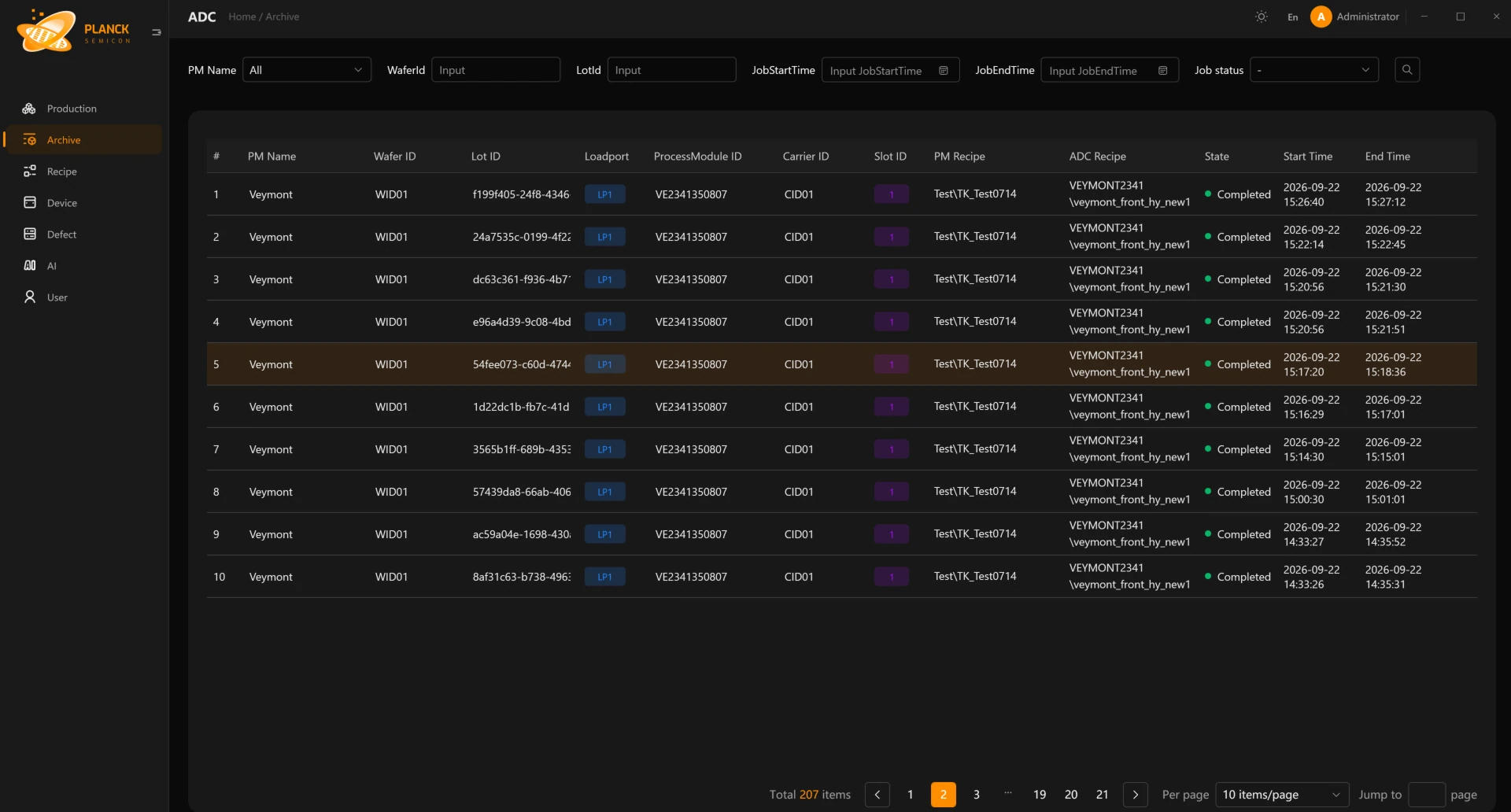
PlanckADC classifies and grades defects automatically, with SPC and Wafer Map traceability.
01MODULAR PLATFORM
Modular Design
01One EFEM
One EFEM,many chambers
One EFEM docks several different inspection and metrology chambers; an EFEM with more load ports takes more chambers, configured to what the line needs.
02One load
One load,all done
The wafer leaves its cassette once: inspection and metrology are completed in the same tool.
03Any mix
Any function,any mix
04One system
One system,lower cost
Shared automation, unified software and common spares save cleanroom space and labor; operators learn it once.
9 SERIES · ANY MIX
Nine platform series · any inspection or metrology function
026 steps × 9 platforms
Process steps × platform coverage
- Main application
- Optional / by configuration
| Process step | Inspection7 | Metrology2 | Platforms | |||||||
|---|---|---|---|---|---|---|---|---|---|---|
| KIBOUnpatterned | ACONCAPatterned | CANIGOBackside | MUSHIWafer edge | CARPPAProcess control | VEYMONTNano-topography | DRAKENSSiC defects | NANSIMulti-channel | ELBRUSWafer geometry | ||
| Incoming Substrate / Wafer QC | 7 | |||||||||
| Epitaxy (Epi) | 4 | |||||||||
| Lithography·Etch·Thin Film | 6 | |||||||||
| CMP·Thinning | 7 | |||||||||
| Advanced Packaging: RDL·Bump·TSV·Bonding·Glass Substrate | 6 | |||||||||
| Outgoing QC·Tool & Process Cleanliness Monitoring | 7 | |||||||||
| Reach | 5 / 6 | 3 / 6 | 5 / 6 | 4 / 6 | 3 / 6 | 4 / 6 | 3 / 6 | 5 / 6 | 5 / 6 | |
| Platform | Incoming Substrate / Wafer QC | Epitaxy (Epi) | Lithography·Etch·Thin Film | CMP·Thinning | Advanced Packaging: RDL·Bump·TSV·Bonding·Glass Substrate | Outgoing QC·Tool & Process Cleanliness Monitoring | Reach |
|---|---|---|---|---|---|---|---|
| Inspection7 | |||||||
| KIBOUnpatterned | 5 / 6 | ||||||
| ACONCAPatterned | 3 / 6 | ||||||
| CANIGOBackside | 5 / 6 | ||||||
| MUSHIWafer edge | 4 / 6 | ||||||
| CARPPAProcess control | 3 / 6 | ||||||
| VEYMONTNano-topography | 4 / 6 | ||||||
| DRAKENSSiC defects | 3 / 6 | ||||||
| Metrology2 | |||||||
| NANSIMulti-channel | 5 / 6 | ||||||
| ELBRUSWafer geometry | 5 / 6 | ||||||
| Platforms | 7 | 4 | 6 | 7 | 6 | 7 | |
03SOFTWARE & PLATFORM
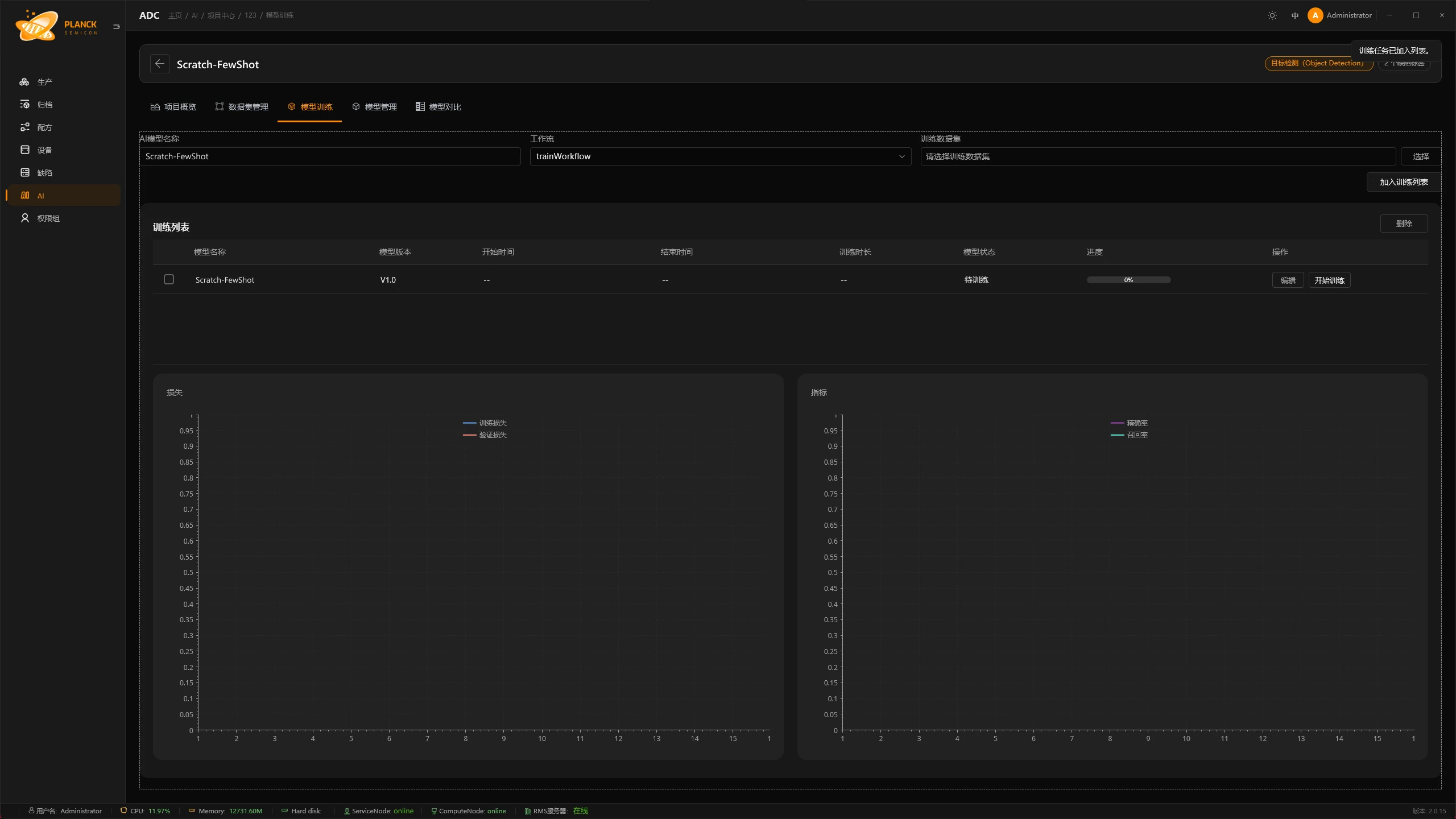
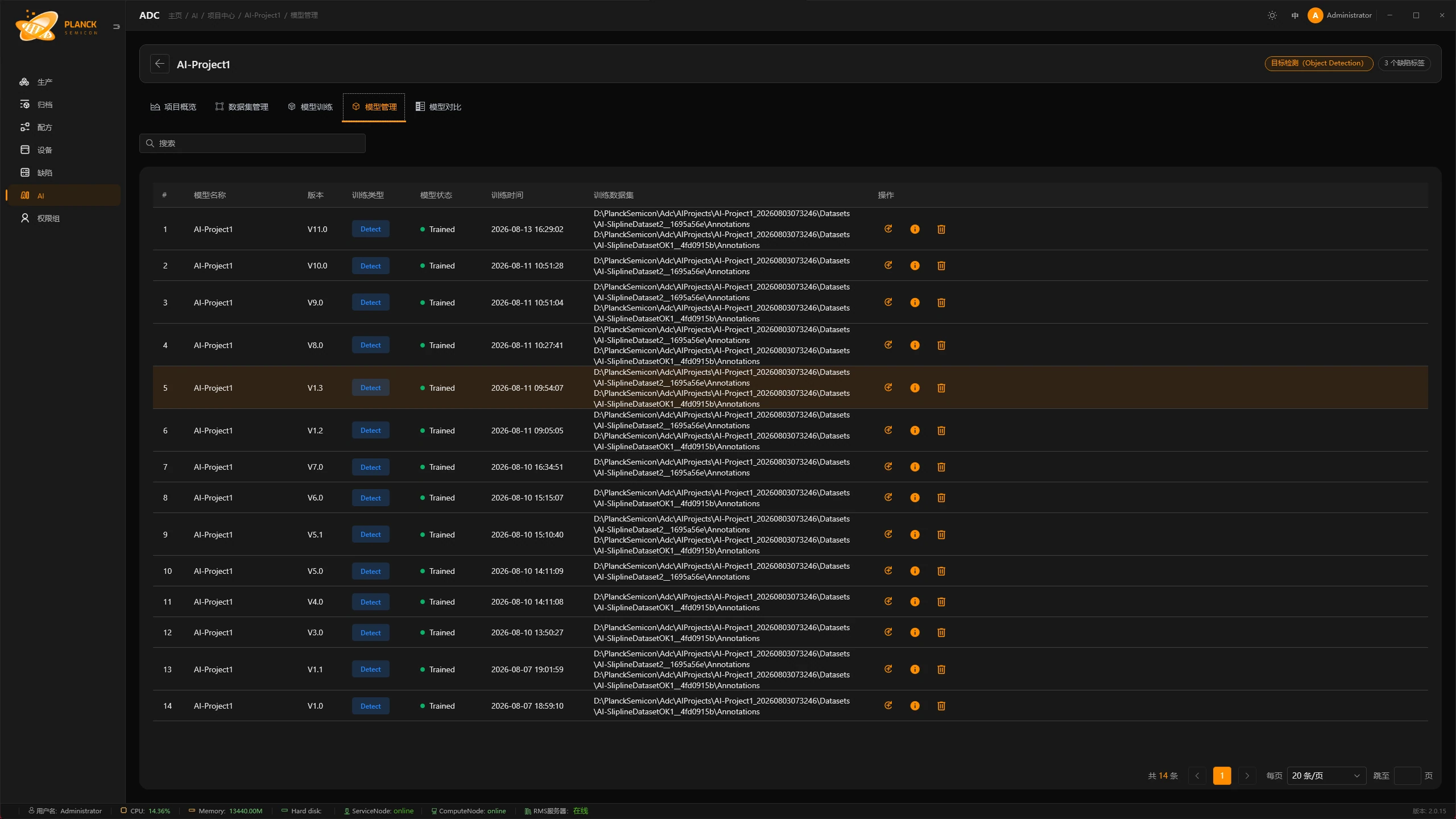
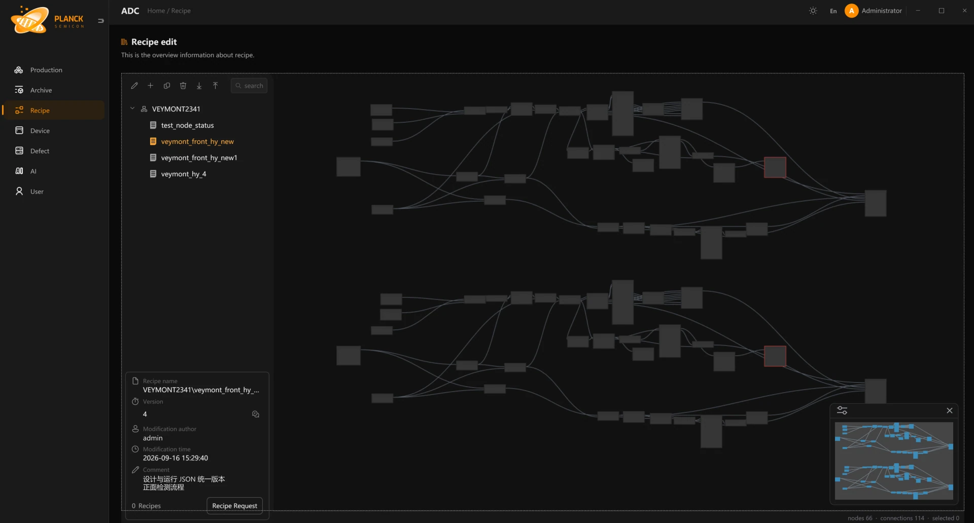
PlanckADC AI defect classification and yield management

START A CONVERSATION
Turn process datainto value
- SalesProducts and commercial inquiriessales@plancksemicon.com
- GeneralCorporate affairs and partnershipsinfo@plancksemicon.com
- Head office
- 11/F, Block B, Long Guang Century Building, Bao’an Center, Bao’an District, Shenzhen, China
- Phone
- +86-755-21063549