
Platform series no. 07/ 09
INSPECTION SERIES
DRAKENS Series
SiC Wafer Surface & Crystal Defect Inspection System Series
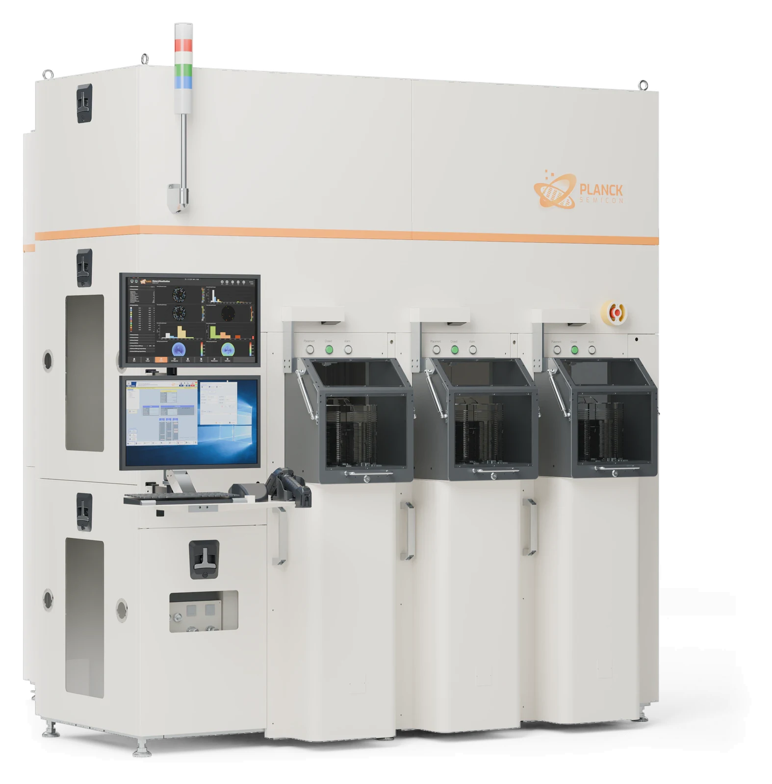
Born for SiC. Ready for more.
- Micro-scratchFaint surface scratches detected
Hard to see in conventional bright-field
- Crystal defectsMicropipes · Dislocations · Polytypes · Stacking faults
Automatic classification and grading
- 12-inchSiC volume inspection
Front and back in one scan · Non-contact backside
01PRODUCT INTRODUCTION
Overview
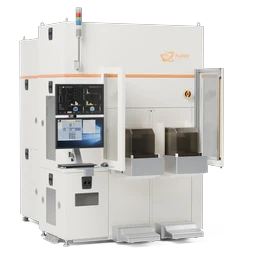
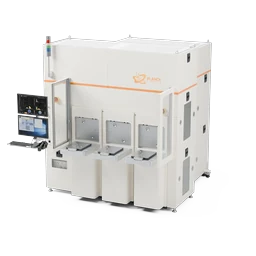
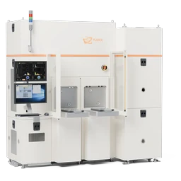
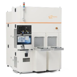
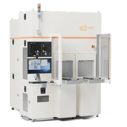
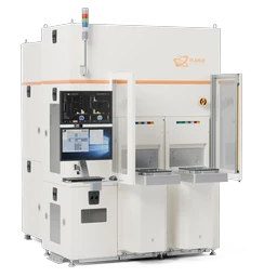
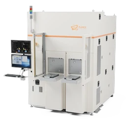
DRAKENS provides fully automatic defect inspection for SiC substrates and epitaxial wafers. A single scan captures front and back together, detecting macro defects such as cracks, edge chips, polishing residue and stains, faint surface scratches that conventional bright-field misses, and crystal defects including micropipes, dislocations, polytype inclusions and stacking faults, all classified and graded automatically. Transparent substrates are held on a non-contact backside support, and the system is ready for 12-inch SiC volume inspection. The same platform also inspects silicon, GaN and other materials.
Inspection targets
- Faint scratches
- Cracks / edge chips
- Polishing residue / stains
- Micropipes
- Dislocations
- Polytypes / stacking faults
Applications
- SiC substrates
- SiC epi wafers
- GaN / compound semiconductors
- Silicon wafer macro inspection
02PRODUCT FEATURES
Key features
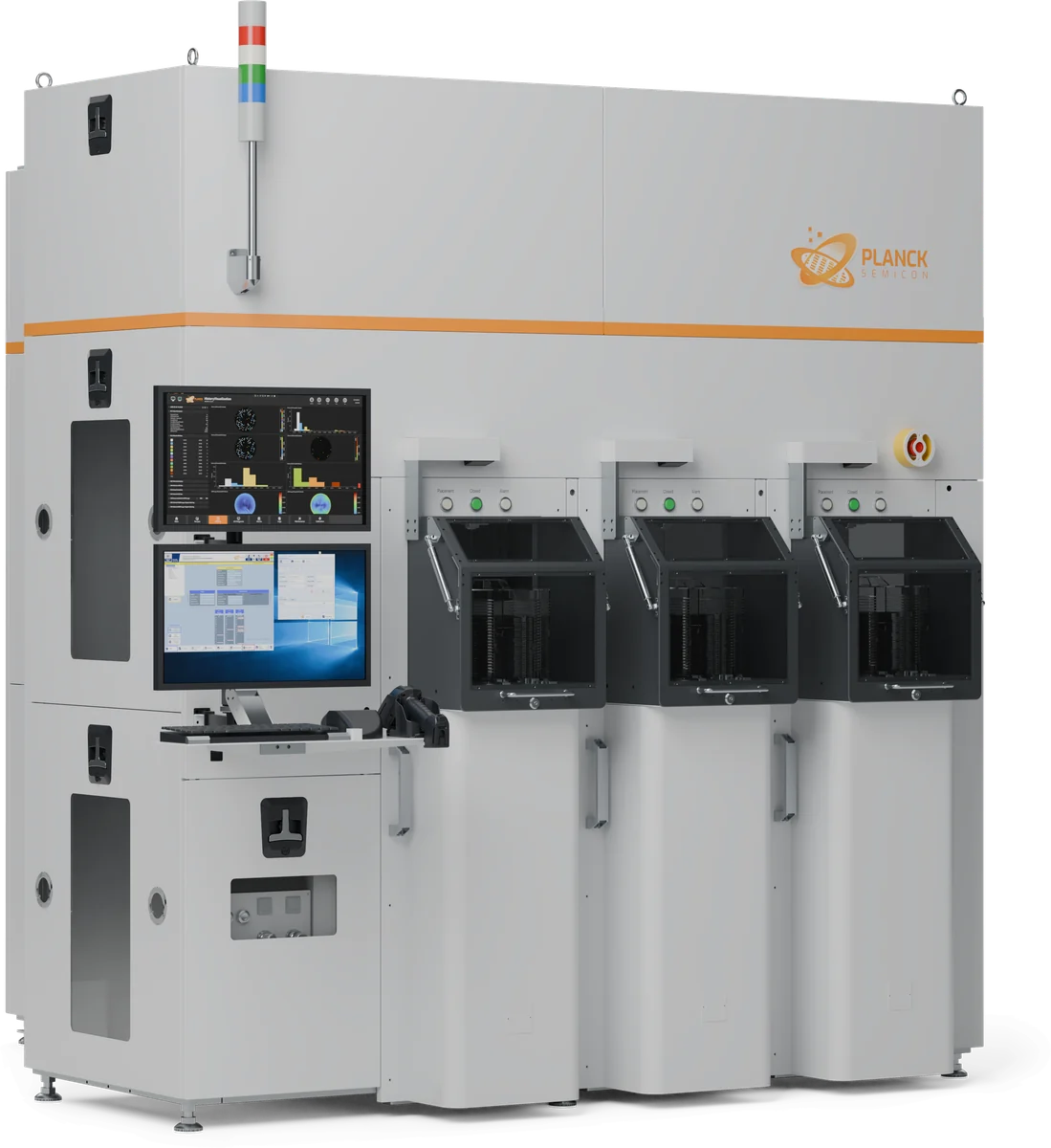
Faint scratches, clearly seen
Faint scratches and polishing marks that conventional bright-field cannot see are clearly detected.
Crystal defects on the same tool
Micropipes, dislocations, polytype inclusions, stacking faults and macro defects in a single scan, classified and graded automatically.
12-inch · Dual-side · Non-contact
Front and back in a single scan, with non-contact backside support for transparent wafers. Silicon and GaN work just as well.
PLANCKADC · Yield-management ready
Results flow straight into PlanckADC
AI classification and grading, result monitoring with SPC, and Wafer Map traceability, connected to your MES / YMS.
About PlanckADC03MORE SYSTEMS
Other systems
- KIBO SeriesUnpatterned Wafer Defect Inspection SystemInspection
- ACONCA SeriesFully Automatic Patterned Wafer Optical Inspection SystemInspection
- CANIGO SeriesAutomatic Wafer Backside Inspection SystemInspection
- MUSHI SeriesAutomatic Wafer Edge Inspection & Metrology SystemInspection
- CARPPA SeriesFast Inline Process Control SystemInspection
- VEYMONT SeriesFull-Surface Nano-Topography Inspection SystemInspection
- NANSI SeriesMulti-Channel Wafer Metrology SystemMetrology
- ELBRUS SeriesFull-Wafer Geometry Metrology SystemMetrology
PRODUCT INQUIRY
Discuss yourprocess needs
We match a platform to your material, process step and the parameters you care about.
- SalesProducts and commercial inquiriessales@plancksemicon.com
- GeneralCorporate affairs and partnershipsinfo@plancksemicon.com
- Head office
- 11/F, Block B, Long Guang Century Building, Bao’an Center, Bao’an District, Shenzhen, China
- Phone
- +86-755-21063549