
Platform series no. 01/ 09
INSPECTION SERIES
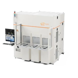
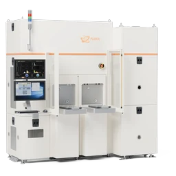
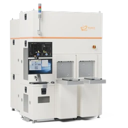
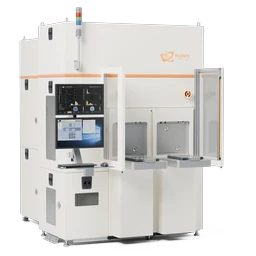
KIBO Series
Unpatterned Wafer Defect Inspection System Series
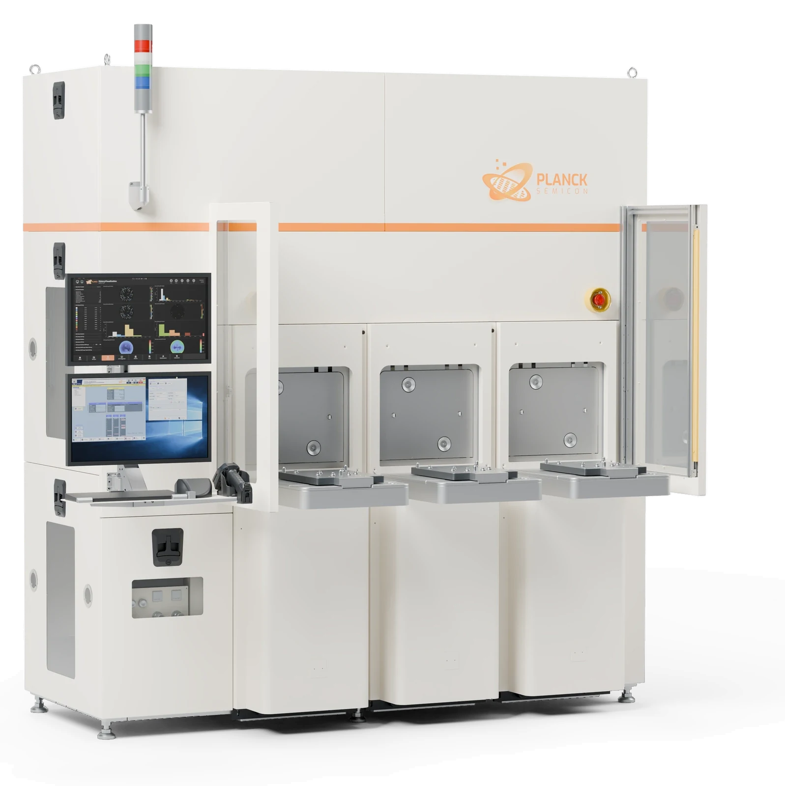
Purity, proven.
- 1x nmTop particle sensitivity
Spot-scan to line-scan models, from the μm range down to 1x nm
- Any substrateTransparent and opaque alike
Si · SiC · GaN · Sapphire · Glass
- Auto-classifyCount · Locate · Bin
Particles · Scratches · Haze · Wafer Map output
01PRODUCT INTRODUCTION
Overview
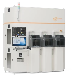
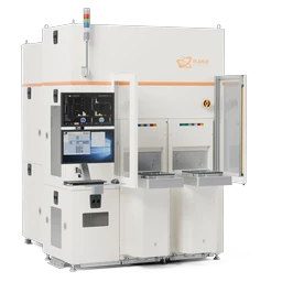
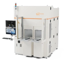
KIBO is a fully automatic unpatterned wafer defect inspection (particle inspection) series. It scans bare silicon, epi, oxide, nitride and metal surfaces across the full wafer at high speed, counting, locating and automatically classifying particles, scratches, haze and other defects. Models range from line-scan to spot-scan, covering sensitivity requirements from the μm range down to 1x nm. Transparent and opaque substrates, including silicon, SiC, GaN, sapphire and glass, are inspected on one platform, for wafer-supplier OQC, fab incoming IQC, and process and tool cleanliness monitoring.
Inspection targets
- Particles
- Scratches
- Haze
- Pits
- COP
Applications
- Silicon wafer IQC / OQC
- Epi wafers
- SiC / GaN substrates
- Glass substrates
- Process and tool contamination monitoring
02PRODUCT FEATURES
Key features
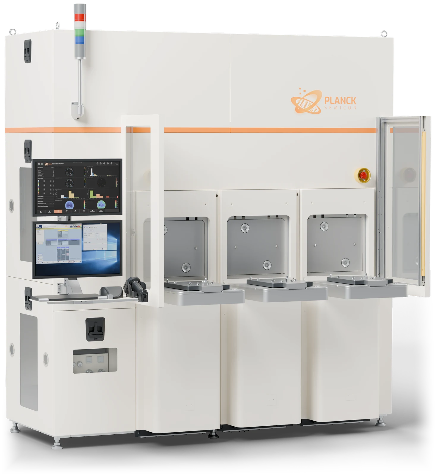
Plug-and-play on the line
SECS/GEM communication, industry-standard result files and automatic binning connect directly to your existing yield systems.
Transparent or opaque
Silicon, SiC, GaN, sapphire and glass inspected on one platform.
Spot-scan and line-scan models
Line-scan models lead on throughput and spot-scan models on sensitivity, covering the μm range down to 1x nm.
PLANCKADC · Yield-management ready
Results flow straight into PlanckADC
AI classification and grading, result monitoring with SPC, and Wafer Map traceability, connected to your MES / YMS.
About PlanckADC03MORE SYSTEMS
Other systems
- ACONCA SeriesFully Automatic Patterned Wafer Optical Inspection SystemInspection
- CANIGO SeriesAutomatic Wafer Backside Inspection SystemInspection
- MUSHI SeriesAutomatic Wafer Edge Inspection & Metrology SystemInspection
- CARPPA SeriesFast Inline Process Control SystemInspection
- VEYMONT SeriesFull-Surface Nano-Topography Inspection SystemInspection
- DRAKENS SeriesSiC Wafer Surface & Crystal Defect Inspection SystemInspection
- NANSI SeriesMulti-Channel Wafer Metrology SystemMetrology
- ELBRUS SeriesFull-Wafer Geometry Metrology SystemMetrology
PRODUCT INQUIRY
Discuss yourprocess needs
We match a platform to your material, process step and the parameters you care about.
- SalesProducts and commercial inquiriessales@plancksemicon.com
- GeneralCorporate affairs and partnershipsinfo@plancksemicon.com
- Head office
- 11/F, Block B, Long Guang Century Building, Bao’an Center, Bao’an District, Shenzhen, China
- Phone
- +86-755-21063549