
Platform series no. 02/ 09
INSPECTION SERIES
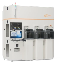
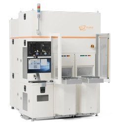
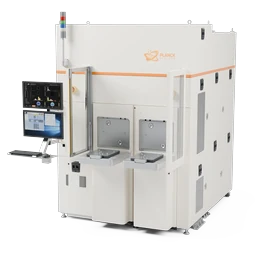
ACONCA Series
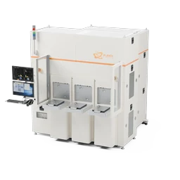
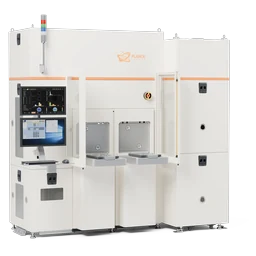
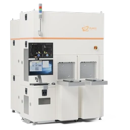
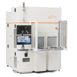
Fully Automatic Patterned Wafer Optical Inspection System Series
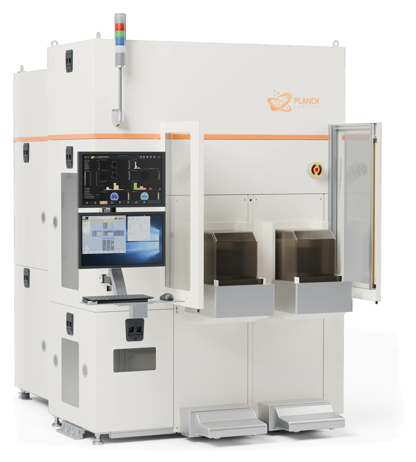
Every side. Every wafer. Zero compromise.
- 2D AOIPattern defects, as standard
PAD · Metal lines · RDL / Bump
- 3D AOI · PLOptional capabilities
3D bump inspection for advanced packaging · Organic residue detection
- Wide-fieldIn-house optics, faster scans
Higher throughput at the same resolution
01PRODUCT INTRODUCTION
Overview
ACONCA is a fully automatic optical inspection (AOI) series for patterned wafers. In-house wide-field optics with bright-field / dark-field illumination inspect the full wafer for PAD corrosion, metal residue, foreign material, scratches, edge chipping, photoresist residue and RDL / bump pattern defects, classify them automatically and output a die-level defect map. An optional 3D AOI module adds 3D inspection of advanced-packaging bumps and pillars, and an optional PL channel finds organic residue on bumps and PADs that bright-field and dark-field cannot see. Square glass substrates and high-warpage wafers are supported. Used in front-end fabs, advanced packaging and 100% inspection of patterned power-device wafers.
Inspection targets
- PAD corrosion
- Metal residue
- Foreign material / scratches
- Edge chipping
- Photoresist residue
- RDL / Bump
- Organic residue (PL)
Applications
- Front-end fab process monitoring
- Advanced packaging RDL / Bump / Pillar
- TGV glass substrates
- Patterned power-device wafers
- Pre-bond Bump / PAD residue (PL)
02PRODUCT FEATURES
Key features
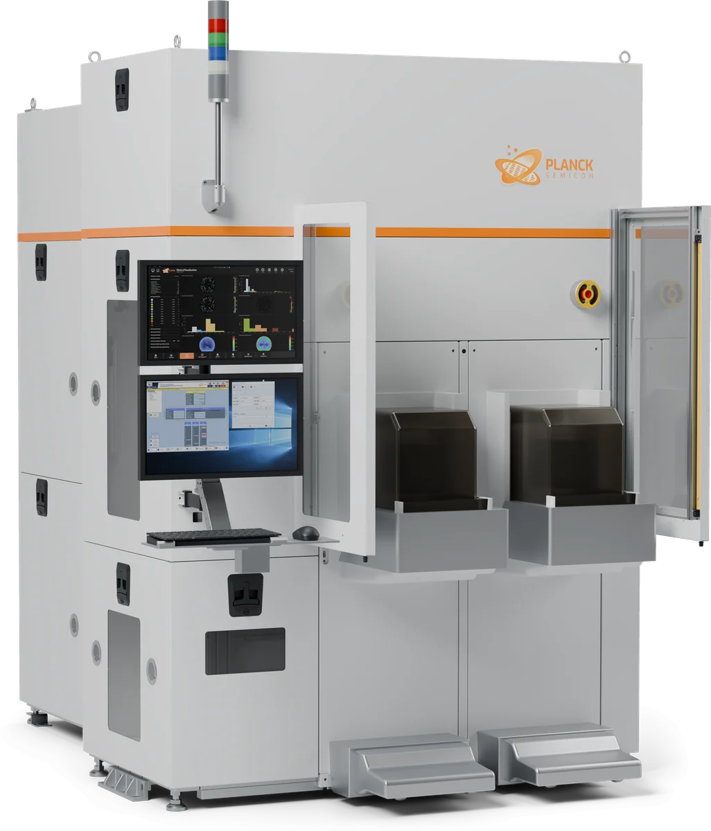
In-house wide-field optics
A larger field of view per frame means less stitching and faster scans at the same resolution.
Optional 3D AOI and PL channels
3D AOI inspects advanced-packaging bumps and pillars in three dimensions; the PL channel detects organic residue on bumps and PADs.
Smart classification and Die Map
ADC classifies defects automatically, and die-level defect maps feed directly into MES / YMS.
PLANCKADC · Yield-management ready
Results flow straight into PlanckADC
AI classification and grading, result monitoring with SPC, and Wafer Map traceability, connected to your MES / YMS.
About PlanckADC03MORE SYSTEMS
Other systems
- KIBO SeriesUnpatterned Wafer Defect Inspection SystemInspection
- CANIGO SeriesAutomatic Wafer Backside Inspection SystemInspection
- MUSHI SeriesAutomatic Wafer Edge Inspection & Metrology SystemInspection
- CARPPA SeriesFast Inline Process Control SystemInspection
- VEYMONT SeriesFull-Surface Nano-Topography Inspection SystemInspection
- DRAKENS SeriesSiC Wafer Surface & Crystal Defect Inspection SystemInspection
- NANSI SeriesMulti-Channel Wafer Metrology SystemMetrology
- ELBRUS SeriesFull-Wafer Geometry Metrology SystemMetrology
PRODUCT INQUIRY
Discuss yourprocess needs
We match a platform to your material, process step and the parameters you care about.
- SalesProducts and commercial inquiriessales@plancksemicon.com
- GeneralCorporate affairs and partnershipsinfo@plancksemicon.com
- Head office
- 11/F, Block B, Long Guang Century Building, Bao’an Center, Bao’an District, Shenzhen, China
- Phone
- +86-755-21063549