
Platform series no. 09/ 09
METROLOGY SERIES
ELBRUS Series
Full-Wafer Geometry Metrology System Series
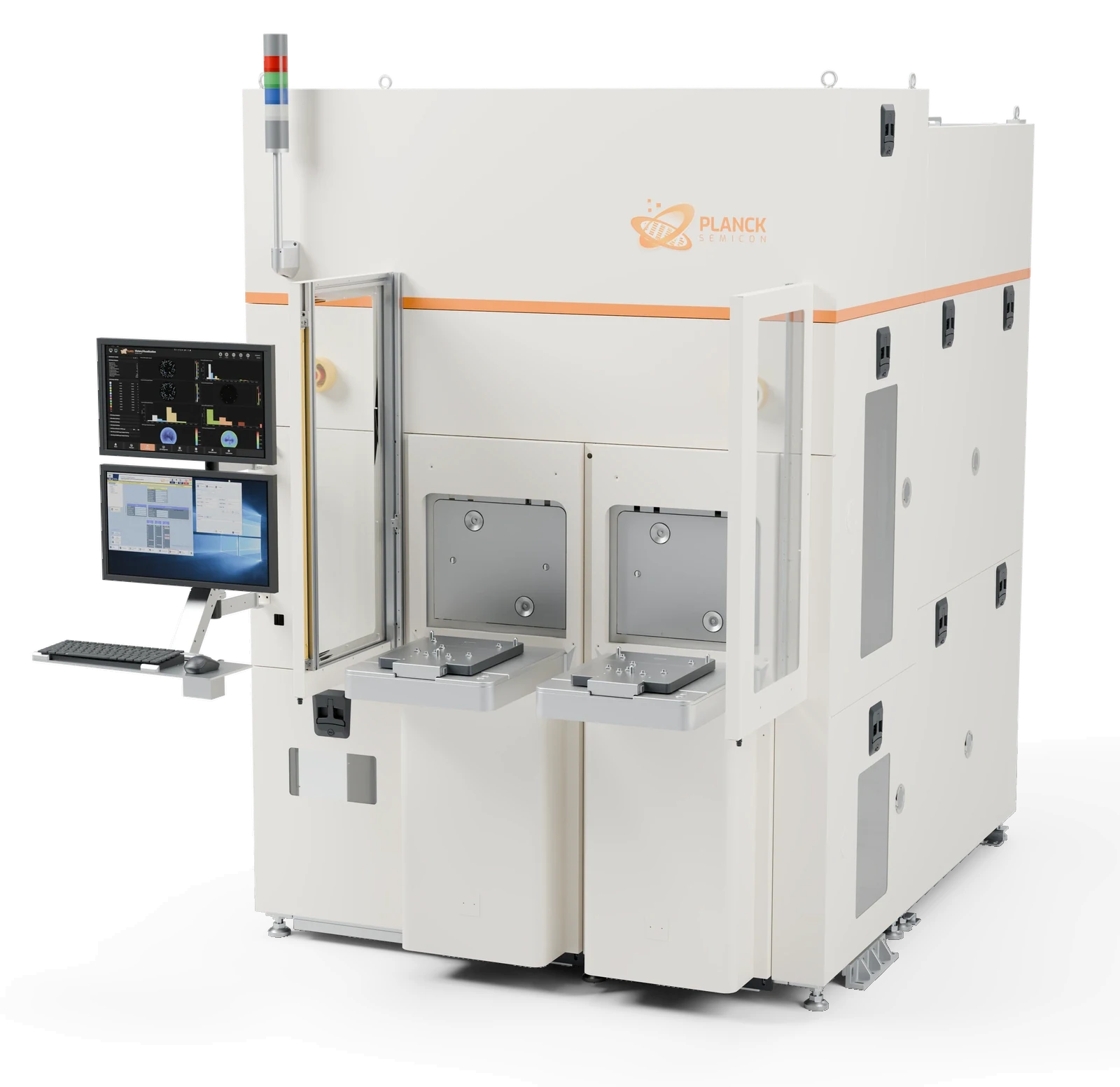
The whole wafer, at once.
- Single shotThe full wafer, no scanning
100% inline in volume production
- Bow · WarpThickness / TTV · Flatness
Reported to SEMI standard definitions
- One recipePatterned and bare wafers on one platform
Bonded · Thinned · High-warpage
01PRODUCT INTRODUCTION
Overview
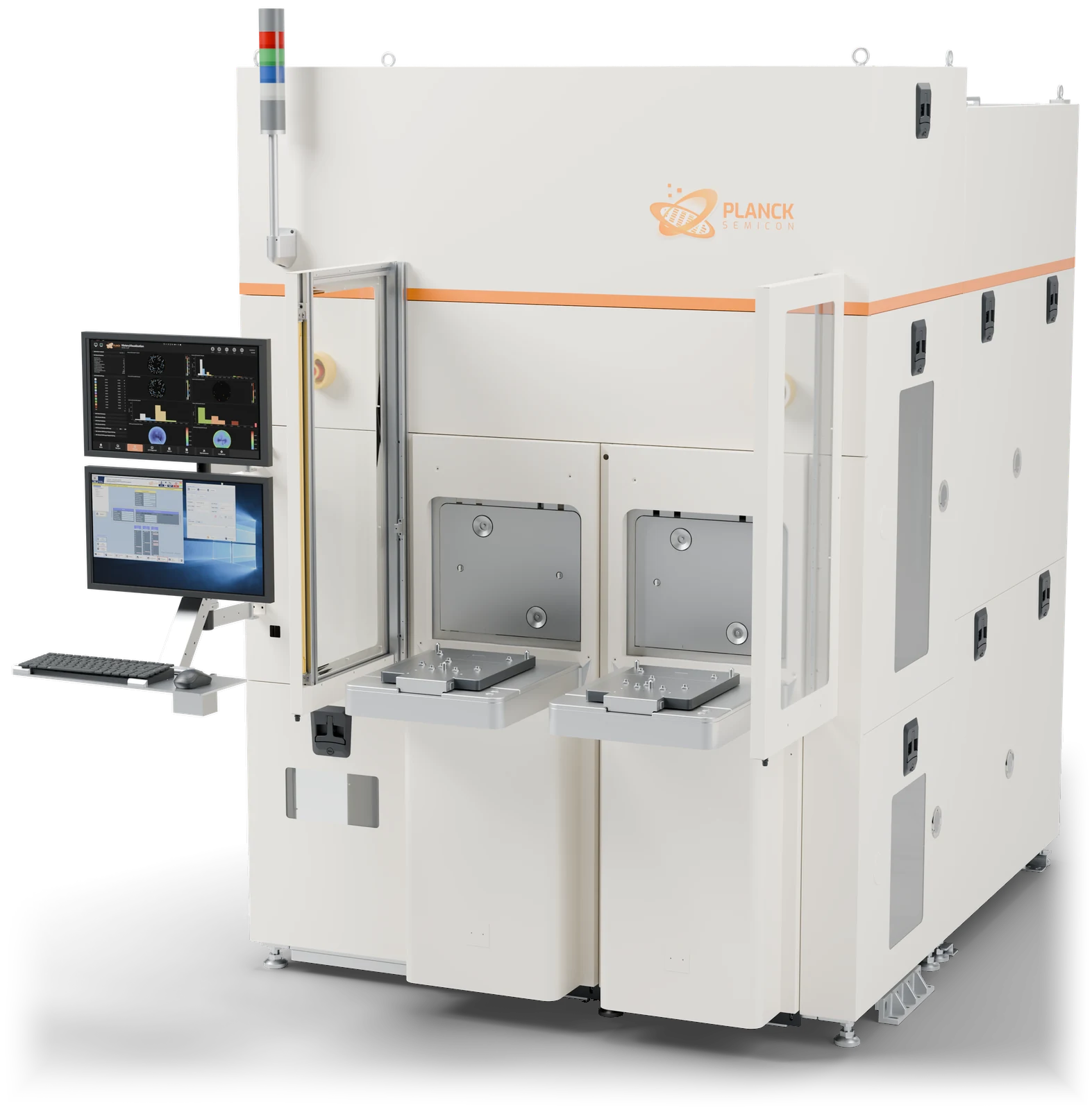
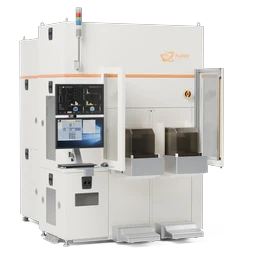
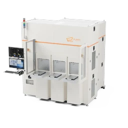
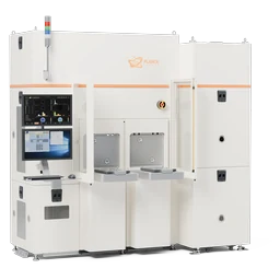
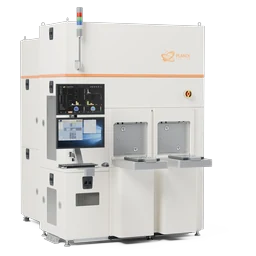
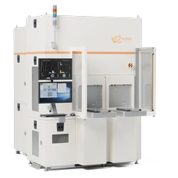
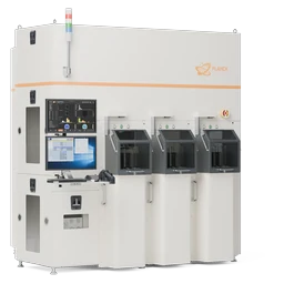
ELBRUS delivers full-wafer geometry metrology for 300 mm patterned and bare wafers. Instead of point-by-point scanning, a single capture yields Bow, Warp, thickness / TTV, flatness and low-to-mid-frequency topography for the entire wafer, fast enough for 100% inline measurement in volume production. Patterned and bare wafers share one recipe system, and bonded, thinned and high-warpage wafers can all be measured. Used for pre-litho geometry control, bonding and thinning process monitoring, CMP stress monitoring and incoming geometry sorting.
Measurements
- Bow / Warp
- Thickness / TTV
- Flatness
- Low-to-mid-frequency topography
Applications
- Pre-litho geometry control
- Bonding / thinning / CMP stress
- Advanced packaging wafer warpage
- Silicon wafer IQC / OQC geometry sorting
02PRODUCT FEATURES
Key features
Single shot, no scanning
The whole wafer captured at once, with no scanning and no stitching, so 100% inline measurement never becomes a bottleneck.
Patterned and bare wafers alike
Patterned, bare, bonded, thinned and high-warpage wafers on the same platform and the same recipe system.
Early warning for litho and bonding
Geometry data correlated with litho focus / overlay and with bonding and thinning stress; non-contact and built for volume production.
PLANCKADC · Yield-management ready
Results flow straight into PlanckADC
AI classification and grading, result monitoring with SPC, and Wafer Map traceability, connected to your MES / YMS.
About PlanckADC03MORE SYSTEMS
Other systems
- KIBO SeriesUnpatterned Wafer Defect Inspection SystemInspection
- ACONCA SeriesFully Automatic Patterned Wafer Optical Inspection SystemInspection
- CANIGO SeriesAutomatic Wafer Backside Inspection SystemInspection
- MUSHI SeriesAutomatic Wafer Edge Inspection & Metrology SystemInspection
- CARPPA SeriesFast Inline Process Control SystemInspection
- VEYMONT SeriesFull-Surface Nano-Topography Inspection SystemInspection
- DRAKENS SeriesSiC Wafer Surface & Crystal Defect Inspection SystemInspection
- NANSI SeriesMulti-Channel Wafer Metrology SystemMetrology
PRODUCT INQUIRY
Discuss yourprocess needs
We match a platform to your material, process step and the parameters you care about.
- SalesProducts and commercial inquiriessales@plancksemicon.com
- GeneralCorporate affairs and partnershipsinfo@plancksemicon.com
- Head office
- 11/F, Block B, Long Guang Century Building, Bao’an Center, Bao’an District, Shenzhen, China
- Phone
- +86-755-21063549